


Integrated Device Technology Inc IDT54FCT162344ETE, IDT54FCT162344ETEB, IDT54FCT162344ETPA, IDT54FCT162344ETPAB, IDT54FCT162344ETPFB Datasheet
...
FAST CMOS ADDRESS/ IDT54/74FCT162344AT/CT/ET
CLOCK DRIVER
Integrated Device Technology, Inc.
FEATURES:
•0.5 MICRON CMOS Technology
•Ideal for address line driving and clock distribution
•8 banks with 1:4 fanout and 3-state
•Typical tSK(o) (Output Skew) < 500ps
•Balanced Output Drivers: ±24mA (commercial),
±16mA (military)
•Reduced system switching noise
•ESD > 2000V per MIL-STD-883, Method 3015;
>200V using machine model (C = 200pF, R = 0)
•Packages include 25 mil pitch SSOP, 19.6 mil pitch TSSOP, 15.7 mil pitch TVSOP and 25 mil pitch Cerpack
•Extended commercial range of -40°C to +85°C
•VCC = 5V ±10%
•Low input and output leakage ≤ 1μA (max.)
DESCRIPTION:
The FCT162344AT/CT/ET is a 1:4 address line driver built using advanced dual metal CMOS technology. This highspeed, low power device provides the ability to fanout to memory arrays. Eight banks, each with a fanout of 4, and 3- state control provide efficient address distribution. One or more banks may be used for clock distribution.
The FCT162344AT/CT/ET has balanced output drive with current limiting resistors. This offers low ground bounce, minimal undershoot and controlled output fall times reducing the need for external series terminating resistors.
A large number of power and ground pins and TTL output swings also ensure reduced noise levels. All inputs are designed with hysteresis for improved noise margins.
FUNCTIONAL BLOCK DIAGRAM
OE1 |
OE3 |
B11 |
B51 |
A1 |
A5 |
B14 |
B54 |
B21 |
B61 |
A2 |
A6 |
B24 |
B64 |
OE2 |
OE4 |
B31 |
B71 |
A3 |
A7 |
B34 |
B74 |
B41 |
B81 |
A4 |
A8 |
B44 |
B84 |
3069 drw 01
The IDT logo is a registered trademark of Integrated Device Technology, Inc.
MILITARY AND COMMERCIAL TEMPERATURE RANGES |
AUGUST 1996 |
||
|
|
|
|
©1996 Integrated Device Technology, Inc. |
5.6 |
DSC-3069/3 |
|
|
|
|
1 |

IDT54/74FCT162344AT/CT/ET |
|
FAST CMOS ADDRESS LINE DRIVER |
MILITARY AND COMMERCIAL TEMPERATURE RANGES |
PIN CONFIGURATIONS
OE1 |
|
1 |
|
56 |
|
OE4 |
B11 |
|
2 |
|
55 |
|
B81 |
|
|
|
||||
B12 |
|
3 |
|
54 |
|
B82 |
|
|
|
||||
GND |
|
4 |
|
53 |
|
GND |
|
|
|
||||
B13 |
|
5 |
|
52 |
|
B83 |
|
|
|
||||
B14 |
|
6 |
|
51 |
|
B84 |
|
|
|
||||
VCC |
|
7 |
|
50 |
|
VCC |
|
|
|
||||
A1 |
|
8 |
|
49 |
|
A8 |
|
|
|
||||
B21 |
|
9 |
|
48 |
|
B71 |
|
|
|
||||
B22 |
|
10 |
|
47 |
|
B72 |
|
|
|
||||
GND |
|
11 |
|
46 |
|
GND |
|
|
|
||||
B23 |
|
12 |
|
45 |
|
B73 |
|
|
|
||||
B24 |
|
13 |
|
44 |
|
B74 |
|
|
|
||||
A2 |
|
14 |
SO56-1 |
43 |
|
A7 |
|
|
|||||
A3 |
|
15 |
SO56-2 |
|
|
|
|
|
|
|
|||
|
SO56-3 |
42 |
|
A6 |
||
B31 |
|
16 |
|
41 |
|
B61 |
|
|
|
||||
B32 |
|
17 |
|
40 |
|
B62 |
|
|
|
||||
GND |
|
18 |
|
39 |
|
GND |
|
|
|
||||
B33 |
|
19 |
|
38 |
|
B63 |
|
|
|
||||
B34 |
|
20 |
|
37 |
|
B64 |
|
|
|
||||
A4 |
|
21 |
|
36 |
|
A5 |
|
|
|
||||
VCC |
|
22 |
|
35 |
|
VCC |
|
|
|
||||
B41 |
|
23 |
|
34 |
|
B51 |
|
|
|
||||
B42 |
|
24 |
|
33 |
|
B52 |
|
|
|
||||
GND |
|
25 |
|
32 |
|
GND |
|
|
|
||||
B43 |
|
26 |
|
31 |
|
B53 |
|
|
|
||||
B44 |
|
27 |
|
30 |
|
B54 |
|
|
|
||||
OE2 |
|
28 |
SSOP/ |
29 |
|
OE3 |
|
|
|||||
|
|
|
|
|
|
|
|
|
TSSOP/TVSOP |
|
|
||
|
|
|
TOP VIEW |
|
3069 drw 02 |
|
OE1 |
|
1 |
|
56 |
|
OE4 |
|
|
|
||||
B11 |
|
2 |
|
55 |
|
B81 |
|
|
|
||||
|
|
|
||||
B12 |
|
3 |
|
54 |
|
B82 |
|
|
|
||||
|
|
|
||||
GND |
|
4 |
|
53 |
|
GND |
|
|
|
||||
|
|
|
||||
B13 |
|
5 |
|
52 |
|
B83 |
|
|
|
||||
|
|
|
||||
B14 |
|
6 |
|
51 |
|
B84 |
|
|
|
||||
|
|
|
||||
VCC |
|
7 |
|
50 |
|
VCC |
|
|
|
||||
|
|
|
||||
A1 |
|
8 |
|
49 |
|
A8 |
|
|
|
||||
|
|
|
||||
B21 |
|
9 |
|
48 |
|
B71 |
|
|
|
||||
|
|
|
||||
B22 |
|
10 |
|
47 |
|
B72 |
|
|
|
||||
|
|
|
||||
GND |
|
11 |
|
46 |
|
GND |
|
|
|
||||
B23 |
|
12 |
|
45 |
|
B73 |
|
|
|
||||
|
|
|
||||
B24 |
|
13 |
|
44 |
|
B74 |
|
|
|
||||
|
|
|
||||
A2 |
|
14 |
E56-1 |
43 |
|
A7 |
|
|
|||||
|
|
|||||
A3 |
|
15 |
|
42 |
|
A6 |
|
|
|
||||
|
|
|
||||
B31 |
|
16 |
|
41 |
|
B61 |
|
|
|
||||
|
|
|
||||
B32 |
|
17 |
|
40 |
|
B62 |
|
|
|
||||
|
|
|
||||
GND |
|
18 |
|
39 |
|
GND |
|
|
|
||||
|
|
|
||||
B33 |
|
19 |
|
38 |
|
B63 |
|
|
|
||||
|
|
|
||||
B34 |
|
20 |
|
37 |
|
B64 |
|
|
|
||||
|
|
|
||||
A4 |
|
21 |
|
36 |
|
A5 |
|
|
|
||||
|
|
|
||||
VCC |
|
22 |
|
35 |
|
VCC |
|
|
|
||||
|
|
|
||||
B41 |
|
23 |
|
34 |
|
B51 |
|
|
|
||||
|
|
|
||||
B42 |
|
24 |
|
33 |
|
B52 |
|
|
|
||||
|
|
|
||||
GND |
|
25 |
|
32 |
|
GND |
|
|
|
||||
|
|
|
||||
B43 |
|
26 |
|
31 |
|
B53 |
|
|
|
||||
|
|
|
||||
B44 |
|
27 |
|
30 |
|
B54 |
|
|
|
||||
OE2 |
|
28 |
|
29 |
|
OE3 |
|
|
|
CERPACK
TOP VIEW
3069 drw 03
5.6 |
2 |
IDT54/74FCT162344AT/CT/ET |
|
FAST CMOS ADDRESS LINE DRIVER |
MILITARY AND COMMERCIAL TEMPERATURE RANGES |
|
|
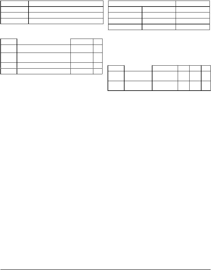
PIN DESCRIPTION |
FUNCTION TABLE(1) |
Pin Names |
Description |
OEx |
3–State Output Enable Inputs (Active LOW) |
Ax |
Inputs |
Bxx |
3-State Outputs |
|
3069 tbl 01 |
ABSOLUTE MAXIMUM RATINGS(1)
Symbol |
Description |
Max. |
Unit |
VTERM(2) |
Terminal Voltage with Respect to |
–0.5 to +7.0 |
V |
|
GND |
|
|
VTERM(3) |
Terminal Voltage with Respect to |
–0.5 to |
V |
|
GND |
VCC +0.5 |
|
|
|
|
|
TSTG |
Storage Temperature |
–65 to +150 |
°C |
IOUT |
DC Output Current |
–60 to +120 |
mA |
NOTES: |
|
3069 lnk 03 |
|
1.Stresses greater than those listed under ABSOLUTE MAXIMUM RATINGS may cause permanent damage to the device. This is a stress rating only and functional operation of the device at these or any other conditions above those indicated in the operational sections of this specification is not implied. Exposure to absolute maximum rating conditions for extended periods may affect reliability.
2.All device terminals except FCT162XXXT Output and I/O terminals.
3.Output and I/O terminals for FCT162XXXT.
Inputs |
|
Outputs |
OEx |
Ax |
Bxx |
L |
L |
L |
L |
H |
H |
H |
X |
Z |
NOTE: |
|
3069 tbl 02 |
1.H = HIGH Voltage Level X = Don’t Care
L = LOW Voltage Level Z = High Impedance
CAPACITANCE (TA = +25°C, f = 1.0MHz)
Symbol |
Parameter(1) |
Conditions |
Typ. |
Max. |
Unit |
CIN |
Input |
VIN = 0V |
3.5 |
6.0 |
pF |
|
Capacitance |
|
|
|
|
COUT |
Output |
VOUT = 0V |
3.5 |
8.0 |
pF |
|
Capacitance |
|
|
|
|
NOTE: |
|
|
|
3069 lnk 04 |
|
1. This parameter is measured at characterization but not tested.
5.6 |
3 |
 Loading...