


Integrated Device Technology Inc IDT49FCT805AD, IDT49FCT805ADB, IDT49FCT805AE, IDT49FCT805AEB, IDT49FCT805AL Datasheet
...FAST CMOS |
IDT49FCT805/A |
BUFFER/CLOCK DRIVER |
IDT49FCT806/A |
Integrated Device Technology, Inc.
FEATURES:
•0.5 MICRON CMOS Technology
•Guaranteed low skew < 700ps (max.)
•Low duty cycle distortion < 1ns (max.)
•Low CMOS power levels
•TTL compatible inputs and outputs
•Rail-to-rail output voltage swing
•High drive: -24mA IOH, 64mA IOL
•Two independent output banks with 3-state control
•1:5 fanout per bank
•‘Heartbeat’ monitor output
•Available in DIP, SOIC, SSOP (805 only), QSOP (805 only), Cerpack and LCC packages
•Military product compliant to MIL-STD-883, Class B
DESCRIPTION:
The IDT49FCT805/A and IDT49FCT806/A are clock drivers built using advanced dual metal CMOS technology. The IDT49FCT805/A is a non-inverting clock driver and the IDT49FCT806/A is an inverting clock driver. Each device consists of two banks of drivers. Each bank drives five output buffers from a standard TTL compatible input. The devices feature a "heartbeat" monitor for diagnostics and PLL driving. The MON output is identical to all other outputs and complies with the output specifications in this document. The IDT49FCT805/A and IDT49FCT806/A offer low capacitance inputs with hysteresis. Rail-to-rail output swing improves noise margin and allows easy interface with CMOS inputs.
FUNCTIONAL BLOCK DIAGRAMS
IDT49FCT805 |
|
|
IDT49FCT806 |
|
|
OEA |
|
|
OEA |
|
|
INA |
5 |
OA1-OA5 |
INA |
5 |
OA1-OA5 |
|
|
||||
INB |
5 |
OB1-OB5 |
INB |
5 |
OB1-OB5 |
|
|
||||
OEB |
|
|
OEB |
|
|
|
|
MON |
|
|
MON |
|
|
2574 drw 01 |
|
|
2574 drw 02 |
The IDT logo is a registered trademark of Integrated Device Technology, Inc.
MILITARY AND COMMERCIAL TEMPERATURE RANGES |
SEPTEMBER 1996 |
|
©1996 Integrated Device Technology, Inc. |
9.1 |
DSC-2574/10 |
1
IDT49FCT805/806/A
FAST CMOS BUFFER/CLOCK DRIVER
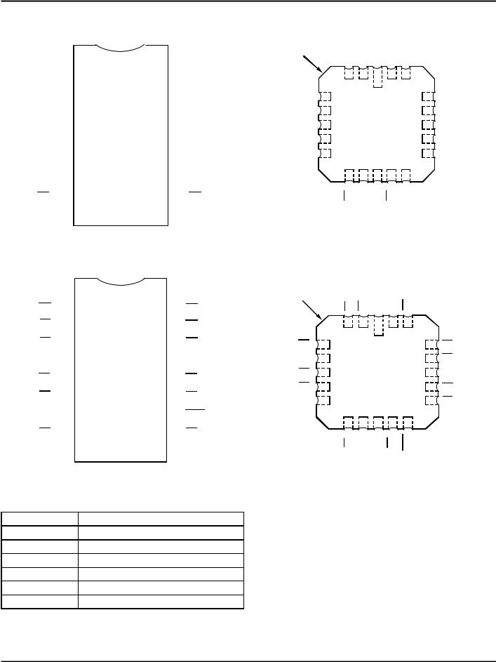
PIN CONFIGURATIONS
IDT49FCT805
VCCA |
|
|
1 |
|
20 |
|
|
|
|
VCCB |
|
OA1 |
|
|
2 |
|
19 |
|
|
|
|
OB1 |
|
|
|
|
|
|
|
|
|||||
OA2 |
|
|
3 |
|
18 |
|
|
|
|
OB2 |
|
|
|
|
|
|
|
|
|||||
OA3 |
|
|
4 |
P20-1 |
17 |
|
|
|
|
OB3 |
|
|
|
|
|
|
|||||||
|
|
|
|
|
D20-1 |
|
|
|
|
|
|
|
|
|
|
|
|
|
|
|
|
|
|
GNDA |
|
|
5 |
SO20-2 |
16 |
|
|
|
|
GNDB |
|
|
|
|
|
|
|
||||||
|
|
|
|
|
SO20-7 |
|
|
|
|
|
|
|
|
|
|
|
|
|
|
|
|
|
|
OA4 |
|
|
6 |
SO20-8 |
15 |
|
|
|
|
OB4 |
|
|
|
|
|
|
|
||||||
|
|
& |
|
|
|
|
|||||
|
|
|
|
|
|
|
|
|
|
|
|
OA5 |
|
|
7 |
E20-1 |
14 |
|
|
|
|
OB5 |
|
|
|
|
|
|
|
||||||
|
|
|
|
|
|
|
|||||
NC(1) |
|
|
8 |
|
13 |
|
|
|
|
MON |
|
|
|
|
|
|
|
|
|||||
OEA |
|
|
9 |
|
12 |
|
|
|
|
OEB |
|
|
|
|
|
|
|
|
|||||
INA |
|
|
10 |
|
11 |
|
|
|
|
INB |
|
|
|
|
|
|
|
|
|||||
|
|
DIP/SOIC/SSOP/QSOP/CERPACK |
|||||||||
|
|
|
|
|
TOP VIEW |
|
|
|
|
2574 drw 03 |
|
IDT49FCT806 |
|
|
|
|
|
|
|
|
|
||
VCCA |
|
|
1 |
|
20 |
|
|
|
|
VCCB |
|
|
|
|
|
|
|
|
|||||
OA1 |
|
|
2 |
|
19 |
|
|
|
|
OB1 |
|
|
|
|
|
|
|
|
|||||
OA2 |
|
|
3 |
|
18 |
|
|
|
|
OB2 |
|
|
|
|
|
|
|
|
|||||
OA3 |
|
|
4 |
P20-1 |
17 |
|
|
|
|
OB3 |
|
|
|
|
|
|
|
||||||
|
|
|
|
|
|
|
|
|
|
|
|
GNDA |
|
|
5 |
D20-1 |
16 |
|
|
|
|
GNDB |
|
|
|
|
|
|
|
||||||
|
|
|
|
|
SO20-2 |
|
|
|
|
|
|
|
|
|
|
|
|
|
|
|
|
|
|
OA4 |
|
|
6 |
& |
15 |
|
|
|
|
OB4 |
|
|
|
|
|
|
|
||||||
|
|
E20-1 |
|
|
|
|
|||||
OA5 |
|
|
7 |
14 |
|
|
|
|
OB5 |
||
|
|
|
|
|
|
|
|||||
|
|
|
|
|
|
|
|||||
NC (1) |
|
|
8 |
|
13 |
|
|
|
|
MON |
|
|
|
|
|
|
|
|
|||||
OEA |
|
|
9 |
|
12 |
|
|
|
|
OEB |
|
|
|
|
|
|
|
|
|||||
INA |
|
|
10 |
|
11 |
|
|
|
|
INB |
|
|
|
|
|
|
|
|
|||||
|
|
|
|
DIP/SOIC/CERPACK |
|
|
|
||||
|
|
|
|
|
TOP VIEW |
|
|
|
2574 drw 05 |
||
PIN DESCRIPTION |
|
|
|
|
|
|
|
||||
Pin Names |
|
|
Description |
||||||||
OEA, OEB |
|
3-State Output Enable Inputs (Active LOW) |
|||||||||
INA, INB |
|
Clock Inputs |
|
|
|
|
|
|
|||
OAn, OBn |
|
Clock Outputs (FCT805) |
|
|
|
||||||
OAn, OBn |
|
Clock Outputs (FCT806) |
|
|
|
||||||
MON |
|
Monitor Output (FCT805) |
|
|
|
||||||
MON |
|
Monitor Output (FCT806 |
|
|
|
||||||
NOTE: |
|
|
|
|
|
|
|
|
2574 tbl 01 |
||
1.Pin 8 is not internally connected on devices with a "K" prefix in the date code. On older devices, pin 8 is internally connected to GND. To insure compatibility with all products, pin 8 should be connected to GND at the board level.
MILITARY AND COMMERCIAL TEMPERATURE RANGES
INDEX |
OA2 |
OA1 |
VCCA |
VCCB |
OB1 |
|
|
|
|
|
|
|
|
|
3 |
2 |
1 |
20 |
19 |
|
OA3 |
4 |
|
|
18 |
OB2 |
|
|
|
|
||||
GNDA |
5 |
|
|
|
17 |
OB3 |
OA4 |
6 |
L20-2 |
|
16 |
GNDB |
|
OA5 |
7 |
|
|
|
15 |
OB4 |
NC(1) |
8 |
|
|
|
14 |
OB5 |
|
9 |
10 |
11 12 |
13 |
|
|
|
OEA |
INA |
INB |
OEB |
MON |
|
|
|
LCC |
|
|
|
|
TOP VIEW |
2574 drw 04 |
|
INDEX |
OA2 |
OA1 |
VCCA |
VCCB |
OB1 |
|
|
|
|||||
|
3 |
2 |
1 |
20 |
19 |
|
OA3 |
4 |
|
|
18 |
OB2 |
|
|
|
|
||||
GNDA |
5 |
|
|
|
17 |
OB3 |
OA4 |
6 |
L20-2 |
|
16 |
GNDB |
|
OA5 |
7 |
|
|
|
15 |
OB4 |
NC(1) |
8 |
|
|
|
14 |
OB5 |
|
9 |
10 |
11 |
12 |
13 |
|
|
OEA |
INA |
INB |
OEB |
MON |
|
|
|
|
LCC |
|
|
|
TOP VIEW |
2574 drw 06 |
|
9.1 |
2 |

IDT49FCT805/806/A |
|
FAST CMOS BUFFER/CLOCK DRIVER |
MILITARY AND COMMERCIAL TEMPERATURE RANGES |
ABSOLUTE MAXIMUM RATINGS(1)
Symbol |
Description |
Max. |
Unit |
VTERM(2) |
Terminal Voltage with Respect to |
–0.5 to +7.0 |
V |
|
GND |
|
|
VTERM(3) |
Terminal Voltage with Respect to |
–0.5 to |
V |
|
GND |
VCC +0.5 |
|
TSTG |
Storage Temperature |
–65 to +150 |
°C |
IOUT |
DC Output Current |
–60 to +120 |
mA |
NOTES: |
|
2574 lnk 03 |
|
1.Stresses greater than those listed under ABSOLUTE MAXIMUM RATINGS may cause permanent damage to the device. This is a stress rating only and functional operation of the device at these or any other conditions above those indicated in the operational sections of this specification is not implied. Exposure to absolute maximum rating conditions for extended periods may affect reliability. No terminal voltage may exceed VCC by +0.5V unless otherwise noted.
2.Input and VCC terminals.
3.Output and I/O terminals.
CAPACITANCE (TA = +25°C, f = 1.0MHz)
Symbol  Parameter(1)
  Conditions
  Typ.
Typ.  Max.
Max.  Unit
Unit
CIN |
Input |
VIN = 0V |
4.5 |
6.0 |
pF |
|
Capacitance |
|
|
|
|
COUT |
Output |
VOUT = 0V |
5.5 |
8.0 |
pF |
|
Capacitance |
|
|
|
|
NOTE: |
|
|
|
2574 lnk 04 |
|
1. This parameter is measured at characterization but not tested.
FUNCTION TABLE(1)
|
|
|
Outputs |
|
|
|
Inputs |
49FCT805 |
49FCT806 |
||
OEA, OEB INA, INB |
OAn, OBn |
MON |
OAn, OBn |
MON |
|
L |
L |
L |
L |
H |
H |
L |
H |
H |
H |
L |
L |
H |
L |
Z |
L |
Z |
H |
H |
H |
Z |
H |
Z |
L |
NOTE: |
|
|
|
|
2574 tbl 02 |
1. H = HIGH, L = LOW, Z = High Impedance
DC ELECTRICAL CHARACTERISTICS OVER OPERATING RANGE
Following Conditions Apply Unless Otherwise Specified: VLC = 0.2V; VHC = VCC – 0.2V
Commercial: TA = 0°C to +70°C, VCC = 5.0V ± 5%; Military: TA = –55°C to +125°C, VCC = 5.0V ± 10%
Symbol |
Parameter |
Test Conditions(1) |
Min. |
Typ.(2) |
Max. |
Unit |
|
VIH |
Input HIGH Level |
Guaranteed Logic HIGH Level |
2.0 |
— |
— |
V |
|
VIL |
Input LOW Level |
Guaranteed Logic LOW Level |
— |
— |
0.8 |
V |
|
II H |
Input HIGH Current(5) |
VCC = Max. |
VI = VCC |
— |
— |
±1 |
μA |
II L |
Input LOW Current(5) |
VCC = Max. |
VI = GND |
— |
— |
±1 |
μA |
IOZH |
Off State (HIGH Z)(5) |
VCC = Max. |
VO = VCC |
— |
— |
±1 |
μA |
IOZL |
Output Current(5) |
|
VO = GND |
— |
— |
±1 |
μA |
VIK |
Clamp Diode Voltage |
VCC = Min., IIN= –18mA |
|
— |
–0.7 |
–1.2 |
V |
IOS |
Short Circuit Current |
VCC = Max.(3), VO = GND |
–60 |
–120 |
— |
mA |
|
VOH |
Output HIGH Voltage |
VCC = 3V, VIN = VLC or VHC, IOH = –32μA |
VHC |
VCC |
— |
V |
|
|
|
VCC = Min. |
IOH = –300μA |
VHC |
VCC |
— |
|
|
|
VIN = VIH or VIL |
IOH = –12mA MIL. |
3.6 |
4.3 |
— |
|
|
|
|
IOH = –15mA COM'L. |
|
|
|
|
|
|
|
IOH = -24mA MIL. |
2.4 |
3.8 |
— |
|
|
|
|
IOH = -24mA COM'L. |
|
|
|
|
VOL |
Output LOW Voltage |
VCC = 3V, VIN = VLC or VHC, IOL= 300μA |
— |
GND |
VLC |
V |
|
|
|
VCC = Min. |
IOH = 300μA |
— |
GND |
VLC(4) |
|
|
|
VIN = VIH or VIL |
IOL = 48mA MIL. |
— |
0.3 |
0.55 |
|
|
|
|
IOL = 64mA COM'L. |
|
|
|
|
VH |
Input Hysteresis for all inputs |
|
— |
— |
200 |
— |
mV |
ICC |
Quiescent Power Supply Current |
VCC = Max., VIN = GND or VCC |
— |
5 |
500 |
μA |
|
NOTES: |
|
|
|
|
|
|
2574 tbl 05 |
1.For conditions shown as Max. or Min., use appropriate value specified under Electrical Characteristics for the applicable device type.
2.Typical values are at VCC = 5.0V, +25°C ambient.
3.Not more than one output should be shorted at one time. Duration of the short circuit test should not exceed one second.
4.This parameter is guaranteed but not tested.
5.The test limit for this parameter is ± 5μA at TA = –55°C.
9.1 |
3 |
 Loading...