


Integrated Device Technology Inc IDT70825L35GB, IDT70825L35PF, IDT70825L35PFB, IDT70825L45G, IDT70825L45GB Datasheet
...
HIGH-SPEED 8K x 16 |
IDT70825S/L |
SEQUENTIAL ACCESS |
|
RANDOM ACCESS MEMORY (SARAM™) |
|
Integrated Device Technology, Inc.
FEATURES:
•8K x 16 Sequential Access Random Access Memory (SARAM™)
-Sequential Access from one port and standard Random Access from the other port
-Separate upper-byte and lower-byte control of the Random Access Port
•High-speed operation
-20ns tAA for random access port
-20ns tCD for sequential port
-25ns clock cycle time
•Architecture based on Dual-Port RAM cells
•Electrostatic discharge > 2001V, Class II
•Compatible with Intel BMIC and 82430 PCI Set
•Width and Depth Expandable
•Sequential side
-Address based flags for buffer control
-Pointer logic supports two internal buffers
•Battery backup operation—2V data retention
•TTL-compatible, single 5V (±10%) power supply
•Available in 80-pin TQFP and 84-pin PGA
•Military product compliant to MIL-STD-883.
•Industrial temperature range (–40°C to +85°C) is available, tested to military electrical specifications.
DESCRIPTION:
The IDT70825 is a high-speed 8K x 16-bit Sequential Access Random Access Memory (SARAM). The SARAM offers a single-chip solution to buffer data sequentially on one port, and be accessed randomly (asynchronously) through the other port. The device has a Dual-Port RAM based architecture with a standard SRAM interface for the random (asynchronous) access port, and a clocked interface with counter sequencing for the sequential (synchronous) access port.
Fabricated using CMOS high-performance technology, this memory device typically operates on less than 900mW of power at maximum high-speed clock-to-data and Random Access. An automatic power down feature, controlled by CE, permits the on-chip circuitry of each port to enter a very low standby power mode.
The IDT70825 is packaged in a 80-pin Thin Plastic Quad Flatpack (TQFP) or 84-pin Ceramic Pin Grid Array (PGA). Military grade product is manufactured in compliance with the latest revision of MIL-STD-883, Class B, making it ideally suited to military temperature applications demanding the highest level of performance and reliability.
FUNCTIONAL BLOCK DIAGRAM
A0-12 |
13 |
|
|
|
SCLK |
|
|
|
|
|
|
|
|
Random |
|
Sequential |
|
R/ |
|
Access |
|
Access |
1 |
|
Port |
|
Port |
||
|
LSB |
|
2 |
||
|
MSB |
Controls |
|
Controls |
|
|
|
8K X 16 |
|
|
|
|
|
|
|
SR/ |
|
|
|
|
Memory |
|
|
|
|
|
|
|
|
|
|
|
Array |
|
|
I/O0-15 |
16 |
16 |
16 |
SI/O0-15 |
|
DataL |
DataR |
Reg. |
|||
|
|
13 |
|
13 |
|
|
|
|
|
|
|
|
|
AddrL |
AddrR |
|
|
|
|
13 |
13 |
RST |
|
|
|
|
Pointer/ |
|
|
|
|
|
|
|
|
|
|
13 |
|
Counter |
|
|
|
|
13 |
|
|
Start Address for Buffer #1 |
|
|
|
|
|
|
|
|
|
||
|
|
|
|
|
|
|
|
|
|||
End Address for Buffer #1 |
|
|
|
|
|
|
|
|
|
1 |
|
|
13 |
|
|
|
|
|
|
||||
Start Address for Buffer #2 |
|
|
|
|
COMPARATOR |
|
|
||||
|
|
|
|||||||||
|
|
|
|||||||||
End Address for Buffer #2 |
|
|
|
|
|
|
|
||||
|
|
|
|
|
|
|
|
|
|
||
Flow Control Buffer |
|
|
|
|
|
|
|
|
|
2 |
|
Flag Status |
|
|
|
|
|
|
|
||||
|
|
|
|
|
|
|
|
|
|||
|
|
|
|
|
|
|
|
|
|||
|
|
|
|
|
|
|
|
3016 drw 01 |
|||
The IDT logo is a registered trademark and SARAM is a trademark of Integrated Device Technology, Inc.
MILITARY AND COMMERCIAL TEMPERATURE RANGES |
OCTOBER 1996 |
|
©1996 Integrated Device Technology, Inc. |
For latest information contact IDT’s web site at www.idt.com or fax-on-demand at 408-492-8391. |
DSC-3016/6 |
6.31 |
1 |
IDT70825S/L |
|
HIGH-SPEED 8K x 16 SEQUENTIAL ACCESS RANDOM ACCESS MEMORY |
MILITARY AND COMMERCIAL TEMPERATURE RANGES |
PIN CONFIGURATIONS(1,2)
|
INDEX |
|
|
SI/O2 |
|
SI/O3 |
|
VCC |
|
SI/O4 SI/O5 |
|
SI/O6 |
|
|
SI/O7 |
|
GND |
|
SI/O8 |
|
SI/O9 |
SI/O10 |
SI/O11 |
|
VCC |
|
SI/O12 |
|
SI/O13 |
|
SI/O14 |
|
|
SI/O15 |
|
GND |
|
N/C |
|
A12 |
|
|
|
|||||||||||||||||||||||||||||
|
|
|
|
|
|
|
|
|
|
|
|
|
|
|
|
|
|
|
|
|
|
|
|
|
|
|
|
|
|
|
|
|
|
|
|
|
|
|
|
|
|
|
|
|
|
|
|
|
|
|
|
|
|
|
|
|
|
|
|
|
|
|
|
|
|
|
||||||
|
SI/O1 |
|
|
80 79 |
78 77 76 75 |
74 73 72 |
71 70 69 |
68 67 66 |
65 64 63 62 61 |
|
|
|
A11 |
|||||||||||||||||||||||||||||||||||||||||||||||||||||||||||
|
|
|
1 |
|
|
|
|
|
|
|
|
|
|
|
|
|
|
|
|
|
|
|
|
|
|
|
|
|
|
|
|
|
|
|
|
|
|
|
|
|
|
|
|
|
|
|
|
|
|
|
|
|
|
|
|
|
|
|
|
|
|
|
|
60 |
|
|
||||||
|
|
|
|
|
|
|
|
|
|
|
|
|
|
|
|
|
|
|
|
|
|
|
|
|
|
|
|
|
|
|
|
|
|
|
|
|
|
|
|
|
|
|
|
|
|
|
|
|
|
|
|
|
|
|
|
|
|
|
|
|
|
|
||||||||||
|
SI/O0 |
|
|
2 |
|
|
|
|
|
|
|
|
|
|
|
|
|
|
|
|
|
|
|
|
|
|
|
|
|
|
|
|
|
|
|
|
|
|
|
|
|
|
|
|
|
|
|
|
|
|
|
|
|
|
|
|
|
|
|
|
|
|
|
|
|
59 |
|
|
A10 |
|||
|
|
|
|
|
|
|
|
|
|
|
|
|
|
|
|
|
|
|
|
|
|
|
|
|
|
|
|
|
|
|
|
|
|
|
|
|
|
|
|
|
|
|
|
|
|
|
|
|
|
|
|
|
|
|
|
|
|
|
|
|
|
|
|
|
|
|
|
|
|
|||
|
GND |
|
|
3 |
|
|
|
|
|
|
|
|
|
|
|
|
|
|
|
|
|
|
|
|
|
|
|
|
|
|
|
|
|
|
|
|
|
|
|
|
|
|
|
|
|
|
|
|
|
|
|
|
|
|
|
|
|
|
|
|
|
|
|
|
|
58 |
|
|
A9 |
|||
|
|
|
|
|
|
|
|
|
|
|
|
|
|
|
|
|
|
|
|
|
|
|
|
|
|
|
|
|
|
|
|
|
|
|
|
|
|
|
|
|
|
|
|
|
|
|
|
|
|
|
|
|
|
|
|
|
|
|
|
|
|
|
|
|
|
|||||||
|
N/C |
|
|
4 |
|
|
|
|
|
|
|
|
|
|
|
|
|
|
|
|
|
|
|
|
|
|
|
|
|
|
|
|
|
|
|
|
|
|
|
|
|
|
|
|
|
|
|
|
|
|
|
|
|
|
|
|
|
|
|
|
|
|
|
|
|
57 |
|
|
A8 |
|||
|
|
|
|
|
|
|
|
|
|
|
|
|
|
|
|
|
|
|
|
|
|
|
|
|
|
|
|
|
|
|
|
|
|
|
|
|
|
|
|
|
|
|
|
|
|
|
|
|
|
|
|
|
|
|
|
|
|
|
|
|
|
|
|
|
|
|||||||
|
SCE |
|
|
5 |
|
|
|
|
|
|
|
|
|
|
|
|
|
|
|
|
|
|
|
|
|
|
|
|
|
|
|
|
|
|
|
|
|
|
|
|
|
|
|
|
|
|
|
|
|
|
|
|
|
|
|
|
|
|
|
|
|
|
|
|
|
56 |
|
|
A7 |
|||
|
|
|
|
|
|
|
|
|
|
|
|
|
|
|
|
|
|
|
|
|
|
|
|
|
|
|
|
|
|
|
|
|
|
|
|
|
|
|
|
|
|
|
|
|
|
|
|
|
|
|
|
|
|
|
|
|
|
|
|
|
|
|
|
|
|
|||||||
|
SR/W |
|
|
|
|
|
|
|
|
|
|
|
|
|
|
|
|
|
|
|
|
|
|
|
|
|
|
|
|
|
|
|
|
|
|
|
|
|
|
|
|
|
|
|
|
|
|
|
|
|
|
|
|
|
|
|
|
|
|
|
|
|
|
|
|
|
||||||
|
|
|
6 |
|
|
|
|
|
|
|
|
|
|
|
|
|
|
|
|
|
|
|
|
|
|
|
|
|
|
|
|
|
|
|
|
|
|
|
|
|
|
|
|
|
|
|
|
|
|
|
|
|
|
|
|
|
|
|
|
|
|
|
|
|
55 |
|
|
A6 |
||||
|
|
|
|
|
|
|
|
|
|
|
|
|
|
|
|
|
|
|
|
|
|
|
|
|
|
|
|
|
|
|
|
|
|
|
|
|
|
|
|
|
|
|
|
|
|
|
|
|
|
|
|
|
|
|
|
|
|
|
|
|
|
|
|
|
|
|
|
|
|
|||
|
RST |
|
|
7 |
|
|
|
|
|
|
|
|
|
|
|
|
|
|
|
|
|
|
|
|
|
|
|
|
|
|
|
|
|
|
|
|
|
|
|
|
|
|
|
|
|
|
|
|
|
|
|
|
|
|
|
|
|
|
|
|
|
|
|
|
|
54 |
|
|
A5 |
|||
|
|
|
|
|
|
|
|
|
|
|
|
|
|
|
|
|
|
|
|
|
|
|
|
|
|
|
|
|
|
|
|
|
|
|
|
|
|
|
|
|
|
|
|
|
|
|
|
|
|
|
|
|
|
|
|
|
|
|
|
|
|
|
|
|
|
|||||||
|
SLD |
|
|
|
|
|
|
|
|
|
|
|
|
|
|
|
|
|
|
|
|
|
|
|
|
|
|
|
|
|
|
|
|
|
|
|
|
|
|
|
|
|
|
|
|
|
|
|
|
|
|
|
|
|
|
|
|
|
|
|
|
|
|
|
|
|
|
|
|
|
||
|
|
|
8 |
|
|
|
|
|
|
|
|
|
|
|
|
|
|
|
|
|
|
|
|
|
|
|
|
|
|
|
|
|
|
|
|
|
|
|
|
|
|
|
|
|
|
|
|
|
|
|
|
|
|
|
|
|
|
|
|
|
|
|
|
|
53 |
|
|
A4 |
||||
|
|
|
|
|
|
|
|
|
|
|
|
|
|
|
|
|
|
|
|
|
|
|
|
|
|
|
|
|
|
|
|
|
|
|
|
|
|
|
|
|
|
|
|
|
|
|
|
|
|
|
|
|
|
|
|
|
|
|
|
|
|
|
|
|
|
|
||||||
SSTRT2 |
|
|
9 |
|
|
|
|
|
|
|
|
|
|
|
|
|
|
|
|
|
|
|
|
|
|
|
|
|
|
IDT70825 |
|
|
|
|
|
|
|
|
|
|
|
|
|
|
|
|
|
|
|
|
|
|
|
|
|
52 |
|
|
A3 |
|||||||||||||
|
|
|
|
|
|
|
|
|
|
|
|
|
|
|
|
|
|
|
|
|
|
|
|
|
|
|
|
|
|
|
|
|
|
|
|
|
|
|
|
|
|
|
|
|
|
|
|
|
|
|
|
|
|
|
||||||||||||||||||
|
|
|
|
|
|
|
|
|
|
|
|
|
|
|
|
|
|
|
|
|
|
|
|
|
|
|
|
|
|
|
|
|
|
|
|
|
|
|
|
|
|
|
|
|
|
|
|
|
|
|
|
|
|
|||||||||||||||||||
SSTRT1 |
|
|
10 |
|
|
|
|
|
|
|
|
|
|
|
|
|
|
|
|
|
|
|
|
|
|
|
|
|
|
PN80-1 |
|
|
|
|
|
|
|
|
|
|
|
|
|
|
|
|
|
|
|
|
|
|
|
|
|
51 |
|
|
A2 |
|||||||||||||
|
|
|
|
|
|
|
|
|
|
|
|
|
|
|
|
|
|
|
|
|
|
|
|
|
|
|
|
|
|
|
|
|
|
|
|
|
|
|
|
|
|
|
|
|
|
|
|
|
|
|
|
|
|
|
||||||||||||||||||
|
GND |
|
|
11 |
|
|
|
|
|
|
|
|
|
|
|
|
|
|
|
|
|
|
|
|
|
|
|
|
|
|
|
TQFP |
|
|
|
|
|
|
|
|
|
|
|
|
|
|
|
|
|
|
|
|
|
|
|
|
|
50 |
|
|
VCC |
|||||||||||
|
|
|
|
|
|
|
|
|
|
|
|
|
|
|
|
|
|
|
|
|
|
|
|
|
|
|
|
|
|
|
|
|
|
|
|
|
|
|
|
|
|
|
|
|
|
|
|
|
|
|
|
|
|
|
|
|
||||||||||||||||
|
GND |
|
|
12 |
|
|
|
|
|
|
|
|
|
|
|
|
|
|
|
|
|
|
|
|
|
|
|
|
|
|
|
|
|
|
|
|
|
|
|
|
|
|
|
|
|
|
|
|
|
|
|
|
|
|
|
|
49 |
|
|
VCC |
||||||||||||
|
|
|
|
|
|
|
|
|
|
|
|
|
|
|
|
|
|
|
|
|
|
|
|
|
|
|
|
|
|
TOP |
|
|
|
|
|
|
|
|
|
|
|
|
|
|
|
|
|
|
|
|
|
|
|
|
|
|
|
|
|
|||||||||||||
CNTEN |
|
|
13 |
|
|
|
|
|
|
|
|
|
|
|
|
|
|
|
|
|
|
|
|
|
|
|
|
|
|
VIEW(3) |
|
|
|
|
|
|
|
|
|
|
|
|
|
|
|
|
|
|
|
|
|
|
|
|
|
48 |
|
|
A1 |
|||||||||||||
|
|
|
|
|
|
|
|
|
|
|
|
|
|
|
|
|
|
|
|
|
|
|
|
|
|
|
|
|
|
|
|
|
|
|
|
|
|
|
|
|
|
|
|
|
|
|
|
|
|
|
|
|
|
|
||||||||||||||||||
|
SOE |
|
|
|
|
|
|
|
|
|
|
|
|
|
|
|
|
|
|
|
|
|
|
|
|
|
|
|
|
|
|
|
|
|
|
|
|
|
|
|
|
|
|
|
|
|
|
|
|
|
|
|
|
|
|
|
||||||||||||||||
|
|
|
14 |
|
|
|
|
|
|
|
|
|
|
|
|
|
|
|
|
|
|
|
|
|
|
|
|
|
|
|
|
|
|
|
|
|
|
|
|
|
|
|
|
|
|
|
|
|
|
|
|
|
|
|
|
|
|
|
|
|
|
|
|
47 |
|
|
A0 |
|||||
|
SCLK |
|
|
|
|
|
|
|
|
|
|
|
|
|
|
|
|
|
|
|
|
|
|
|
|
|
|
|
|
|
|
|
|
|
|
|
|
|
|
|
|
|
|
|
|
|
|
|
|
|
|
|
|
|
|
|
|
|
|
|
|
|
|
|
|
|
|
|
|
|||
|
|
|
15 |
|
|
|
|
|
|
|
|
|
|
|
|
|
|
|
|
|
|
|
|
|
|
|
|
|
|
|
|
|
|
|
|
|
|
|
|
|
|
|
|
|
|
|
|
|
|
|
|
|
|
|
|
|
|
|
|
|
|
|
|
46 |
|
|
CMD |
|||||
|
|
|
|
|
|
|
|
|
|
|
|
|
|
|
|
|
|
|
|
|
|
|
|
|
|
|
|
|
|
|
|
|
|
|
|
|
|
|
|
|
|
|
|
|
|
|
|
|
|
|
|
|
|
|
|
|
|
|
|
|
|
|
|
|
||||||||
|
GND |
|
|
16 |
|
|
|
|
|
|
|
|
|
|
|
|
|
|
|
|
|
|
|
|
|
|
|
|
|
|
|
|
|
|
|
|
|
|
|
|
|
|
|
|
|
|
|
|
|
|
|
|
|
|
|
|
|
|
|
|
|
|
|
|
45 |
|
|
CE |
||||
|
|
|
|
|
|
|
|
|
|
|
|
|
|
|
|
|
|
|
|
|
|
|
|
|
|
|
|
|
|
|
|
|
|
|
|
|
|
|
|
|
|
|
|
|
|
|
|
|
|
|
|
|
|
|
|
|
|
|
|
|
|
|
|
|
||||||||
|
|
|
|
|
|
|
|
|
|
|
|
|
|
|
|
|
|
|
|
|
|
|
|
|
|
|
|
|
|
|
|
|
|
|
|
|
|
|
|
|
|
|
|
|
|
|
|
|
|
|
|
|
|
|
|
|
|
|
|
|
|
|
44 |
|
|
LB |
||||||
|
EOB2 |
|
|
17 |
|
|
|
|
|
|
|
|
|
|
|
|
|
|
|
|
|
|
|
|
|
|
|
|
|
|
|
|
|
|
|
|
|
|
|
|
|
|
|
|
|
|
|
|
|
|
|
|
|
|
|
|
|
|
|
|
|
|
|
|
|
|
||||||
|
|
|
|
|
|
|
|
|
|
|
|
|
|
|
|
|
|
|
|
|
|
|
|
|
|
|
|
|
|
|
|
|
|
|
|
|
|
|
|
|
|
|
|
|
|
|
|
|
|
|
|
|
|
|
|
|
|
|
|
|
|
|
|
|
||||||||
|
|
|
|
|
|
|
|
|
|
|
|
|
|
|
|
|
|
|
|
|
|
|
|
|
|
|
|
|
|
|
|
|
|
|
|
|
|
|
|
|
|
|
|
|
|
|
|
|
|
|
|
|
|
|
|
|
|
|
|
|
|
|
|
|
||||||||
|
EOB1 |
|
|
18 |
|
|
|
|
|
|
|
|
|
|
|
|
|
|
|
|
|
|
|
|
|
|
|
|
|
|
|
|
|
|
|
|
|
|
|
|
|
|
|
|
|
|
|
|
|
|
|
|
|
|
|
|
|
|
|
|
|
|
|
|
43 |
|
|
UB |
||||
|
|
|
|
|
|
|
|
|
|
|
|
|
|
|
|
|
|
|
|
|
|
|
|
|
|
|
|
|
|
|
|
|
|
|
|
|
|
|
|
|
|
|
|
|
|
|
|
|
|
|
|
|
|
|
|
|
|
|
|
|
|
|
|
|
||||||||
|
VCC |
|
|
19 |
|
|
|
|
|
|
|
|
|
|
|
|
|
|
|
|
|
|
|
|
|
|
|
|
|
|
|
|
|
|
|
|
|
|
|
|
|
|
|
|
|
|
|
|
|
|
|
|
|
|
|
|
|
|
|
|
|
|
|
|
42 |
|
|
R/W |
||||
|
|
|
|
|
|
|
|
|
|
|
|
|
|
|
|
|
|
|
|
|
|
|
|
|
|
|
|
|
|
|
|
|
|
|
|
|
|
|
|
|
|
|
|
|
|
|
|
|
|
|
|
|
|
|
|
|
|
|
|
|
|
|
|
|
||||||||
|
I/O0 |
|
|
20 |
|
|
|
|
|
23 24 |
25 26 27 28 29 30 |
31 32 33 34 35 |
|
|
|
|
|
|
|
|
|
|
|
|
|
|
|
41 |
|
|
OE |
|||||||||||||||||||||||||||||||||||||||||
|
|
|
|
|
|
|
|
|
|
|
|
|
|
|
|
|
|
|
|
|
|
|
|
|
||||||||||||||||||||||||||||||||||||||||||||||||
|
|
|
|
21 22 |
36 37 38 39 40 |
|
|
|
|
|||||||||||||||||||||||||||||||||||||||||||||||||||||||||||||||
|
|
|
|
|
|
|
|
|
|
|
|
|
|
|
|
|
|
|
|
|
|
|
|
|
|
|
|
|
|
|
|
|
|
|
|
|
|
|
|
|
|
|
|
|
|
|
|
|
|
|
|
|
|
|
|
|
|
|
|
|
|
|
|
|||||||||
|
|
|
|
1 |
|
GND |
2 |
3 |
|
CC |
4 |
5 |
6 |
7 |
GND |
8 |
9 |
10 |
|
11 |
CC |
12 |
13 |
14 |
|
15 |
GND |
|
|
|
||||||||||||||||||||||||||||||||||||||||||
|
|
|
|
|
I/O |
|
|
|
|
I/O |
|
|
|
|
|
|
I/O |
I/O |
I/O |
I/O |
|
|
|
|||||||||||||||||||||||||||||||||||||||||||||||||
|
|
|
|
|
I/O |
I/O |
|
V |
I/O |
I/O |
I/O |
I/O |
I/O |
I/O |
I/O |
V |
3016 drw 02 |
|||||||||||||||||||||||||||||||||||||||||||||||||||||||
|
|
|
|
|
|
|
|
|
|
|
|
|
|
|
|
|
|
|
|
|
|
|
|
|
|
|
|
|
|
|
|
|
|
|
||||||||||||||||||||||||||||||||||||||
|
|
|
|
|
|
|
|
|
|
|
|
|
|
|
|
|
|
|
|
|
|
|
|
|
|
|
|
|
|
|
|
|
|
|
|
|
|
|
|
|
|
|
|
|
|
|
|
|
|
|
|
|
|
|
|
|
|
|
|
|
|
|
|
|
|
|
||||||
|
|
|
|
|
|
|
|
|
|
|
|
|
|
|
|
|
|
|
|
|
|
|
|
|
|
|
|
|
|
|
|
|
|
|
|
|
|
|
|
|
|
|
|
|
|
|
|
|
|
|
|
|
|
|
|
|
|
|
|
|
|
|
|
|
|
|
|
|
|
|
|
|
63 |
61 |
|
|
|
|
60 |
|
|
|
|
|
|
58 |
|
|
|
|
|
55 |
|
|
|
|
|
|
54 |
|
|
|
|
51 |
|
|
|
|
|
|
48 |
|
|
|
|
|
|
46 |
|
|
|
|
|
|
45 |
|
|
|
42 |
||||||||||||||||
|
I/O1 |
VCC |
|
|
|
|
|
|
|
|
|
|
GND |
|
|
|
|
|
|
|
|
GND |
SSTRT2 |
|
|
|
|
|
|
|
|
|
|
|
NC |
|
GND |
NC |
||||||||||||||||||||||||||||||||||
|
|
EOB1 |
|
CNTEN |
SR/W |
|
|
|||||||||||||||||||||||||||||||||||||||||||||||||||||||||||||||||
|
|
|
|
|
|
|
|
|
|
|
|
|
|
|
|
|
|
|
|
|
|
|
|
|
|
|
|
|
|
|
|
|
|
|
|
|
|
|
|
|
|
|
|
|
|
|
|
|
|
|
|
|
|
|
|
|
|
|
|
|
|
|
|
|
|
|
|
|
|
|
|
|
66 |
64 |
|
|
|
|
62 |
|
|
|
|
|
|
59 |
|
|
|
|
|
56 |
|
|
|
|
|
|
49 |
|
|
|
|
50 |
|
|
|
|
|
|
47 |
|
|
|
|
|
|
44 |
|
|
|
|
|
43 |
|
|
|
40 |
|||||||||||||||||
|
I/O2 |
NC |
|
|
I/O0 |
|
EOB2 |
|
|
SOE |
|
RST |
|
|
SLD |
|
SCE |
|
|
|
SI/O0 |
|
SI/O1 |
SI/O3 |
||||||||||||||||||||||||||||||||||||||||||||||||
|
|
|
|
|
|
|
|
|
|
|
|
|
|
|
|
|
|
|
|
|
|
|
|
|
|
|
|
|
|
|
|
|
|
|
|
|
|
|
|
|
|
|
|
|
|
|
|
|
|
|
|
|
|
|
|
|
|
|
|
|
|
|
|
|
|
|
|
|
|
|
|
|
67 |
65 |
|
|
|
|
|
|
|
|
|
|
|
|
|
|
|
|
|
|
|
|
|
57 |
|
|
|
|
|
|
53 |
|
|
|
|
52 |
|
|
|
|
|
|
|
|
|
|
|
|
|
|
|
|
|
|
|
|
|
|
|
|
41 |
|
|
|
39 |
||||||||
|
I/O3 |
GND |
|
|
|
|
|
|
|
|
|
|
|
|
|
|
|
|
|
|
SCLK |
GND |
SSTRT1 |
|
|
|
|
|
|
|
|
|
|
|
|
|
|
|
|
|
|
|
SI/O2 |
VCC |
||||||||||||||||||||||||||||
|
|
|
|
|
|
|
|
|
|
|
|
|
|
|
|
|
|
|
|
|
|
|
|
|
|
|
|
|
|
|
|
|
|
|
|
|
|
|
|
|
|
|
|
|
|
|
|
|
|
|
|
|
|
|
|
|
|
|
|
|
|
|
|
|
|
|
|
|
|
|
|
|
69 |
68 |
|
|
|
|
|
|
|
|
|
|
|
|
|
|
|
|
|
|
|
|
|
|
|
|
|
|
|
|
|
|
|
|
|
|
|
|
|
|
|
|
|
|
|
|
|
|
|
|
|
|
|
|
|
|
|
|
|
|
|
|
|
|
38 |
|
|
|
37 |
||||
|
I/O4 |
VCC |
|
|
|
|
|
|
|
|
|
|
|
|
|
|
|
|
|
|
|
|
|
|
|
|
|
|
|
|
|
|
|
|
|
|
|
|
|
|
|
|
|
|
|
|
|
|
|
|
|
|
|
|
|
|
|
|
|
|
SI/O4 |
SI/O5 |
||||||||||
|
|
|
|
|
|
|
|
|
|
|
|
|
|
|
|
|
|
|
|
|
|
|
|
|
|
|
|
|
|
|
|
|
|
|
|
|
|
|
|
|
|
|
|
|
|
|
|
|
|
|
|
|
|
|
|
|
|
|
|
|
|
|
|
|
|
|
|
|
|
|
|
|
72 |
71 |
|
|
|
|
73 |
|
|
|
|
|
|
|
|
|
|
|
|
|
|
|
|
|
|
|
|
|
|
|
|
|
|
|
|
|
|
|
|
|
|
|
|
|
|
|
|
|
|
|
|
|
|
33 |
|
|
|
|
|
35 |
|
|
|
34 |
|||||||||
|
I/O7 |
|
I/O6 |
|
GND |
|
|
|
|
|
|
|
|
|
|
|
|
|
|
IDT70825 |
|
|
|
|
|
|
|
|
|
|
|
|
|
|
|
|
|
SI/O8 |
|
SI/O7 |
GND |
|||||||||||||||||||||||||||||||
|
|
|
|
|
|
|
|
|
|
|
|
|
|
|
|
|
|
|
|
|
|
|
|
|
|
|
|
|
|
|
|
|
|
|
|
|
|
|
|
|
|
|
|
|
|
|
|
|
|
|
|
|
|
|
|
|
|
|
|
|
|
|||||||||||
75 |
70 |
|
|
|
|
74 |
|
|
|
|
|
|
|
|
|
|
|
|
|
|
|
|
|
|
|
|
|
G84-3 |
|
|
|
|
|
|
|
|
|
|
|
|
|
|
|
|
|
|
32 |
|
|
|
|
|
31 |
|
|
|
36 |
|||||||||||||||
|
I/O9 |
I/O5 |
|
|
I/O8 |
|
|
|
|
|
|
|
|
|
|
|
|
|
|
84-PIN PGA |
|
|
|
|
|
|
|
|
|
|
|
|
|
SI/O9 |
SI/O10 |
SI/O6 |
||||||||||||||||||||||||||||||||||||
|
|
|
|
|
|
|
|
|
|
|
|
|
|
|
|
|
|
|
|
|
|
|
|
|
|
|
|
TOP VIEW(3) |
|
|
|
|
|
|
|
|
|
|
|
|
|
|
|
|
|
|
|
|
|
|
|
|
|
|
|
|
||||||||||||||||
76 |
77 |
|
|
|
|
78 |
|
|
|
|
|
|
|
|
|
|
|
|
|
|
|
|
|
|
|
|
|
|
|
|
|
|
|
|
28 |
|
|
|
|
|
29 |
|
|
|
30 |
|||||||||||||||||||||||||||
|
I/O10 |
I/O11 |
|
|
VCC |
|
|
|
|
|
|
|
|
|
|
|
|
|
|
|
|
|
|
|
|
|
|
|
|
|
|
|
|
|
|
|
|
|
|
|
|
|
|
|
|
|
|
|
SI/O12 VCC |
SI/O11 |
||||||||||||||||||||||
|
|
|
|
|
|
|
|
|
|
|
|
|
|
|
|
|
|
|
|
|
|
|
|
|
|
|
|
|
|
|
|
|
|
|
|
|
|
|
|
|
|
|
|
|
|
|
|
|
|
|
|
|
|
|
|
|
|
|
|
|
|
|
|
|
|
|
|
|
|
|
|
|
79 |
80 |
|
|
|
|
|
|
|
|
|
|
|
|
|
|
|
|
|
|
|
|
|
|
|
|
|
|
|
|
|
|
|
|
|
|
|
|
|
|
|
|
|
|
|
|
|
|
|
|
|
|
|
|
|
|
|
|
|
|
|
|
|
|
26 |
|
|
|
27 |
||||
|
I/O12 |
I/O13 |
|
|
|
|
|
|
|
|
|
|
|
|
|
|
|
|
|
|
|
|
|
|
|
|
|
|
|
|
|
|
|
|
|
|
|
|
|
|
|
|
|
|
|
|
|
|
|
|
|
|
|
|
|
|
|
|
|
|
SI/O14 SI/O13 |
|||||||||||
|
|
|
|
|
|
|
|
|
|
|
|
|
|
|
|
|
|
|
|
|
|
|
|
|
|
|
|
|
|
|
|
|
|
|
|
|
|
|
|
|
|
|
|
|
|
|
|
|
|
|
|
|
|
|
|
|
|
|
|
|
|
|
|
|
|
|
|
|
|
|
|
|
81 |
83 |
|
|
|
|
|
|
|
|
|
|
|
|
|
|
|
|
|
|
|
|
7 |
|
|
|
|
|
|
11 |
|
|
|
12 |
|
|
|
|
|
|
|
|
|
|
|
|
|
|
|
|
|
|
|
|
|
|
|
|
23 |
|
|
|
25 |
||||||||||
|
I/O14 |
NC |
|
|
|
|
|
|
|
|
|
|
|
|
|
|
|
|
|
|
CMD |
VCC |
|
|
A2 |
|
|
|
|
|
|
|
|
|
|
|
|
|
|
|
|
|
|
|
|
|
|
|
NC |
SI/O15 |
||||||||||||||||||||||
|
|
|
|
|
|
|
|
|
|
|
|
|
|
|
|
|
|
|
|
|
|
|
|
|
|
|
|
|
|
|
|
|
|
|
|
|
|
|
|
|
|
|
|
|
|
|
|
|
|
|
|
|
|
|
|
|
|
|
|
|
|
|
|
|
|
|
|
|
|
|
|
|
82 |
1 |
|
|
|
|
|
2 |
|
|
|
|
|
|
5 |
|
|
|
|
|
8 |
|
|
|
|
|
|
10 |
|
|
|
14 |
|
|
|
|
|
|
17 |
|
|
|
|
20 |
|
|
|
|
|
|
22 |
|
|
|
24 |
||||||||||||||||||
|
I/O15 |
GND |
|
|
|
OE |
|
|
|
|
|
LB |
|
|
|
A0 |
|
|
|
VCC |
|
|
A4 |
|
|
|
|
|
A7 |
|
|
|
|
A10 |
|
|
A12 |
GND |
||||||||||||||||||||||||||||||||||
|
|
|
|
|
|
|
|
|
|
|
|
|
|
|
|
|
|
|
|
|
|
|
|
|
|
|
|
|
|
|
|
|
|
|
|
|
|
|
|
|
|
|
|
|
|
|
|
|
|
|
|
|
|
|
|
|
|
|
|
|
|
|
|
|
|
|
|
|
|
|
|
|
84 |
3 |
|
|
|
|
|
4 |
|
|
|
|
|
|
6 |
|
|
|
|
|
9 |
|
|
|
|
|
|
15 |
|
|
|
13 |
|
|
|
|
|
|
16 |
|
|
|
|
18 |
|
|
|
|
|
|
19 |
|
|
|
21 |
||||||||||||||||||
|
NC R/W UB CE A1 |
|
|
|
|
|
A5 |
|
|
A3 |
|
|
|
|
|
A6 |
|
|
|
|
A8 |
|
|
|
|
|
A9 |
A11 |
||||||||||||||||||||||||||||||||||||||||||||
11
10
09
08
07
06
05
04
03
02
01
A |
B |
C |
D |
E |
F |
G |
H |
J |
K |
L |
INDEX |
|
|
|
|
|
|
|
|
|
3016 drw 03 |
NOTES:
1.All VCC pins must be connected to power supply.
2.All GND pins must be connected to ground supply.
3.This text does not indicate orientation of the actual part-marking.
6.31 |
2 |

IDT70825S/L |
|
HIGH-SPEED 8K x 16 SEQUENTIAL ACCESS RANDOM ACCESS MEMORY |
MILITARY AND COMMERCIAL TEMPERATURE RANGES |
PIN DESCRIPTIONS: RANDOM ACCESS PORT
SYMBOL |
NAME |
I/O(1) |
DESCRIPTION |
A0-A12 |
Address Lines |
I |
Address inputs to access the 8192-word (16 bit) memory array. |
|
|
|
|
I/O0-I/O15 |
Inputs/Outputs |
I |
Random access data inputs/outputs for 16-bit wide data. |
CE |
Chip Enable |
I |
When CE is LOW, the random access port is enabled. When CE is HIGH, the random access |
|
|
|
port is disabled into power-down mode and the I/O outputs are in the high-impedance state. All |
|
|
|
data is retained during CE = VIH, unless it is altered by the sequential port. CE and CMD may not |
|
|
|
be LOW at the same time. |
CMD |
Control Register |
I |
When CMD is LOW, Address lines A0-A2, R/W, and inputs/outputs I/O0-I/O11, are used to |
|
Enable |
|
access the control register, the flag register, and the start and end of buffer registers. CMD and |
|
|
|
CE may not be LOW at the same time. |
R/W |
Read/Write Enable |
I |
If CE is LOW and CMD is HIGH, data is written into the array when R/W is LOW and read out of the |
|
|
|
array when R/W is HIGH. If CE is HIGH and CMD is LOW, R/W is used to access the buffer com- |
|
|
|
mand registers. CE and CMD may not be LOW at the same time. |
|
|
|
|
OE |
Output Enable |
I |
When OE is LOW and R/W is HIGH, I/O0-I/O15 outputs are enabled. When OE is HIGH, the I/O |
|
|
|
outputs are in the high-impedance state. |
|
|
|
|
LB,UB |
Lower Byte, Upper |
I |
When LB is LOW, I/O0-I/O7 are accessible for read and write operations. When LB is HIGH, I/O0- |
|
Byte Enables |
|
I/O7 are tri-stated and blocked during read and write operations. UB controls access for I/O8- |
|
|
|
I/O15 in the same manner and is asynchronous from LB. |
|
|
|
|
VCC |
Power Supply |
|
Seven +5V power supply pins. All Vcc pins must be connected to the same +5V VCC supply. |
|
|
|
|
GND |
Ground |
|
Ten Ground pins. All Ground pins must be connected to the same Ground supply. |
|
|
|
|
|
|
|
3016 tbl 01 |
PIN DESCRIPTIONS: SEQUENTIAL ACCESS PORT |
|||
SYMBOL |
NAME |
I/O(1) |
DESCRIPTION |
SI/O0-15 |
Inputs |
I/O |
Sequential data inputs/outputs for 16-bit wide data. |
SCLK |
Clock |
I |
SI/O0-SI/O15, SCE, SR/W, and SLD are registered on the LOW-to-HIGH transition of SCLK. |
|
|
|
Also, the sequential access port address pointer increments by 1 on each LOW-to-HIGH |
|
|
|
transition of SCLK when CNTEN is LOW. |
SCE |
Chip Enable |
I |
When SCE is LOW, the sequential access port is enabled on the LOW-to-HIGH transition of |
|
|
|
SCLK. When SCE is HIGH, the sequential access port is disabled into powered-down mode on |
|
|
|
the LOW-to-HIGH transition of SCLK, and the SI/O outputs are in the high-impedance state. All |
|
|
|
data is retained, unless altered by the random access port. |
CNTEN |
Counter Enable |
I |
When CNTEN is LOW, the address pointer increments on the LOW-to-HIGH transition of SCLK. |
|
|
|
This function is independant of SCE. |
SR/W |
Read/Write Enable |
I |
When SR/W and SCE are LOW, a write cycle is initiated on the LOW-to-HIGH transition of |
|
|
|
SCLK. When SR/W is HIGH, and SCE and SOE are LOW, a read cycle is initiated on the |
|
|
|
LOW-to-HIGH transition of SCLK. Termination of a Write cycle is done on the Low-to-High |
|
|
|
transistion of SCLK if SR/W or SCE is High. |
SLD |
Address Pointer |
I |
When SLD is sampled LOW, there is an internal delay of one cycle before the address pointer |
|
Load Control |
|
changes. When SLD is LOW, data on the inputs SI/O0-SI/O11 is loaded into a data-in register |
|
|
|
on the LOW-to-HIGH transition of SCLK. On the cycle following SLD, the address pointer |
|
|
|
changes to the address location contained in the data-in register. SSTRT1 and SSTRT2 may |
|
|
|
not be LOW while SLD is LOW or during the cycle following SLD. |
SSTRT1, |
Load Start of |
I |
When SSTRT1 or SSTRT2 is LOW, the start of address register #1 or #2 is loaded into the |
SSTRT2 |
Address Register |
|
address pointer on the LOW-to-HIGH transition of SCLK. The start addresses are stored in |
|
|
|
internal registers. SSTRT1 and SSTRT2 may not be LOW while SLD is LOW or during the cycle |
|
|
|
following SLD. |
EOB1, |
End of Buffer Flag |
O |
EOB1 or EOB2 is output LOW when the address pointer is incremented to match the address |
EOB2 |
|
|
stored in the end of buffer registers. The flags can be cleared by either asserting RST LOW or |
|
|
|
by writing zero into bit 0 and/or bit 1 of the control register at address 101. EOB1 and EOB2 are |
|
|
|
dependent on separate internal registers, and therefore separate match addresses. |
SOE |
Output Enable |
I |
SOE controls the data outputs and is independent of SCLK. When SOE is LOW, output buffers |
|
|
|
and the sequentially addressed data is output. When SOE is HIGH, the SI/O output bus is in |
|
|
|
the high-impedance state. SOE is asynchronous to SCLK. |
RST |
Reset |
I |
When RST is LOW, all internal registers are set to their default state, the address pointer is set |
|
|
|
to zero and the EOB1 and EOB2 flags are set HIGH. RST is asynchronous to SCLK. |
NOTE: |
|
|
3016 tbl 02 |
1. "I/O" is bidirectional Input and Output. "I" is Input and "O" is Output.
6.31 |
3 |

IDT70825S/L |
|
HIGH-SPEED 8K x 16 SEQUENTIAL ACCESS RANDOM ACCESS MEMORY |
MILITARY AND COMMERCIAL TEMPERATURE RANGES |
ABSOLUTE MAXIMUM RATINGS(1)
Symbol |
Rating |
Commercial |
Military |
Unit |
|
|
|
|
|
VTERM(2) |
Terminal Voltage |
–0.5 to +7.0 |
–0.5 to +7.0 |
V |
|
with Respect |
|
|
|
|
to GND |
|
|
|
|
|
|
|
|
TA |
Operating |
0 to +70 |
–55 to +125 |
°C |
|
Temperature |
|
|
|
|
|
|
|
|
TBIAS |
Temperature |
–55 to +125 |
–65 to +135 |
°C |
|
Under Bias |
|
|
|
|
|
|
|
|
TSTG |
Storage |
–55 to +125 |
–65 to +150 |
°C |
|
Temperature |
|
|
|
|
|
|
|
|
IOUT |
DC Output |
50 |
50 |
mA |
|
Current |
|
|
|
|
|
|
|
|
NOTES: |
|
|
3016 tbl 03 |
|
1.Stresses greater than those listed under ABSOLUTE MAXIMUM RATINGS may cause permanent damage to the device. This is a stress rating only and functional operation of the device at these or any other conditions above those indicated in the operational sections of this specification is not implied. Exposure to absolute maximum rating conditions for extended periods may affect reliability.
2.VTERM must not exceed Vcc + 0.5V for more than 25% of the cycle time or 10ns maximum, and is limited to < 20mA for the period of VTERM > Vcc + 0.5V.
RECOMMENDED OPERATING TEMPERATURE AND SUPPLY VOLTAGE
|
Ambient |
|
|
Grade |
Temperature |
GND |
VCC |
Military |
–55°C to +125°C |
0V |
5.0V ± 10% |
|
|
|
|
Commercial |
0°C to +70°C |
0V |
5.0V ± 10% |
3016 tbl 04
RECOMMENDED DC OPERATING
CONDITIONS
Symbol |
Parameter |
Min. |
Typ. |
Max. |
Unit |
VCC |
Supply Voltage |
4.5 |
5.0 |
5.5 |
V |
|
|
|
|
|
|
GND |
Supply Voltage |
0 |
0 |
0 |
V |
|
|
|
|
|
|
VIH |
Input High Voltage |
2.2 |
— |
6.0(2) |
V |
VIL |
Input Low Voltage |
–0.5(1) |
— |
0.8 |
V |
NOTES: |
|
|
|
3016 tbl 05 |
|
1.VIL > –1.5V for pulse width less than 10ns.
2.VTERM must not exceed Vcc + 0.5V.
CAPACITANCE(1)
(TA = +25°C, F = 1.0MHz)TQFP ONLY
Symbol |
Parameter |
Conditions(2) |
Max. |
|
Unit |
CIN |
Input Capacitance |
VIN = 3dV |
9 |
|
pF |
|
|
|
|
|
|
COUT |
Output |
VOUT = 3dV |
10 |
|
pF |
|
Capacitance |
|
|
|
|
|
|
|
|
|
|
NOTES: |
|
|
|
3016 tbl 06 |
|
1.This parameter is determined by device characterization, but is not production tested.
2. 3dV references the interpolated capacitance when the input and output signals switch from 0V to 3V or from 3V to 0V.
DC ELECTRICAL CHARACTERISTICS OVER THE OPERATING TEMPERATURE AND SUPPLY VOLTAGE RANGE (VCC = 5.0V ± 10%)
|
|
|
IDT70825S |
IDT70825L |
|
||
Symbol |
Parameter |
Test Conditions |
Min. |
Max. |
Min. |
Max. |
Unit |
|
|
|
|
|
|
|
|
|ILI| |
Input Leakage Current(1) |
VCC = Max. VIN = GND to VCC |
— |
5.0 |
— |
1.0 |
μA |
|ILO| |
Output Leakage Current |
VCC = Max. CE and SCE = VIH |
— |
5.0 |
— |
1.0 |
μA |
|
|
VOUT = GND to VCC |
|
|
|
|
|
|
|
|
|
|
|
|
|
VOL |
Output Low Voltage |
IOL = 4mA, VCC = Min. |
— |
0.4 |
— |
0.4 |
V |
|
|
|
|
|
|
|
|
VOH |
Output High Voltage |
IOH = –4mA, VCC = Min. |
2.4 |
— |
2.4 |
— |
V |
|
|
|
|
|
|
|
|
NOTE: |
|
|
|
|
|
|
3016 tbl 07 |
1. At Vcc ≤ 2.0V input leakages are undefined.
6.31 |
4 |

IDT70825S/L |
|
HIGH-SPEED 8K x 16 SEQUENTIAL ACCESS RANDOM ACCESS MEMORY |
MILITARY AND COMMERCIAL TEMPERATURE RANGES |
DC ELECTRICAL CHARACTERISTICS OVER THE OPERATING TEMPERATURE AND SUPPLY VOLTAGE RANGE(1) (VCC = 5.0V ± 10%)
|
|
|
|
|
|
70825X20 |
70825X25 |
70825X35 |
70825X45 |
|
|||||
|
|
Test |
|
|
Com'l. Only |
Com'l. Only |
|
|
|
|
|
||||
Symbol |
Parameter |
Condition |
Version |
Typ.(2) |
Max. |
Typ.(2)Max. |
Typ.(2) |
Max. |
Typ.(2) |
Max. |
Unit |
||||
ICC |
Dynamic Operating |
CE = VIL, Outputs |
MIL. |
S |
— |
|
— |
— |
— |
160 |
400 |
155 |
400 |
mA |
|
|
Current |
Open, SCE = VIL(5) |
|
L |
— |
|
— |
— |
— |
160 |
340 |
155 |
340 |
|
|
|
(Both Ports Active) |
f = fMAX(3) |
COM’L. S |
180 |
|
380 |
170 |
360 |
160 |
340 |
155 |
340 |
|
||
|
|
> |
|
|
L |
180 |
|
330 |
170 |
310 |
160 |
290 |
155 |
290 |
|
|
|
|
|
|
|
|
|
|
|
|
|
|
|
|
|
ISB1 |
Standby Current |
SCE and CE VIH(7) |
MIL. |
S |
— |
|
— |
— |
— |
20 |
85 |
16 |
85 |
mA |
|
|
(Both Ports - TTL Level |
CMD = VIH |
|
L |
— |
|
— |
— |
— |
20 |
65 |
16 |
65 |
|
|
|
Inputs) |
f = fMAX(3) |
|
|
|
|
|
|
|
|
|
|
|
||
|
COM’L. S |
25 |
|
70 |
25 |
70 |
20 |
70 |
16 |
70 |
|
||||
|
|
CE or SCE = VIH |
|
L |
25 |
|
50 |
25 |
50 |
20 |
50 |
16 |
50 |
|
|
ISB2 |
Standby Current |
MIL. |
S |
— |
|
— |
— |
— |
95 |
290 |
90 |
290 |
mA |
||
|
(One Port - TTL Level |
Active Port Outputs |
|
L |
|
|
—— |
— |
— |
95 |
250 |
90 |
250 |
|
|
|
Input) |
Open, f = fMAX(3) |
|
|
|
|
|
|
|
|
|
|
|
|
|
|
|
COM’L. S |
115 |
|
260 |
105 |
250 |
95 |
240 |
90 |
240 |
|
|||
|
|
|
|
|
L |
115 |
|
230 |
105 |
220 |
95 |
210 |
90 |
210 |
|
ISB3 |
Full Standby Current |
Both Ports CE and |
MIL. |
S |
— |
|
— |
— |
— |
1.0 |
30 |
1.0 |
30 |
mA |
|
|
(Both Ports - CMOS |
SCE ³ VCC - 0.2V(6,7) |
|
L |
— |
|
— |
— |
— |
0.2 |
10 |
0.2 |
10 |
|
|
|
Level Inputs) |
VIN ³ VCC - 0.2V or |
COM’L. S |
1.0 |
|
15 |
1.0 |
15 |
1.0 |
15 |
1.0 |
15 |
|
||
|
|
VIN £ 0.2V, f = 0(4) |
|
L |
0.2 |
|
5 |
0.2 |
5 |
0.2 |
5 |
0.2 |
5 |
|
|
ISB4 |
Full Standby Current |
One Port CE or |
MIL. |
S |
— |
|
— |
— |
— |
90 |
260 |
85 |
260 |
mA |
|
|
(One Port - CMOS |
SCE ³ VCC - 0.2V(6) |
|
L |
— |
|
— |
— |
— |
90 |
215 |
85 |
215 |
|
|
|
Level Inputs) |
Outputs Open |
|
|
|
|
|
|
|
|
|
|
|
|
|
|
|
(Active port), f = fMAX(3) |
COM’L. S |
110 |
|
240 |
100 |
230 |
90 |
220 |
85 |
220 |
|
||
|
|
VIN ³ VCC - 0.2V or |
|
|
|
|
|
|
|
|
|
|
|
|
|
|
|
VIN £ 0.2V |
|
L |
110 |
|
200 |
100 |
190 |
90 |
180 |
85 |
180 |
|
|
NOTES: |
|
|
|
|
|
|
|
|
|
|
|
|
|
3016 tbl 08 |
|
1."X" in part number indicates power rating (S or L).
2.VCC = 5V, Ta = +25°C; guaranteed by device characterization but not production tested.
3.At f = fMAX, address, control lines (except Output Enable), and SCLK are cycling at the maximum frequency read cycle of 1/tRC.
4.f = 0 means no address or control lines change.
5.SCE may transition, but is Low (SCE=VIL) when clocked in by SCLK.
6.SCE may be ≤ 0.2V, after it is clocked in, since SCLK=VIH must be clocked in prior to powerdown.
7.If one port is enabled (either CE or SCE = Low) then the other port is disabled (SCE or CE = High, respectively). CMOS High > Vcc - 0.2V and Low < 0.2V, and TTL High = VIH and Low = VIL.
DATA RETENTION CHARACTERISTICS OVER ALL TEMPERATURE RANGES (L VERSION ONLY) (VLC < 0.2V, VHC > VCC - 0.2V)
Symbol |
Parameter |
Test Condition |
Min. |
Typ.(1) |
Max. |
Unit |
|
VDR |
VCC for Data Retention |
VCC = 2V |
|
2.0 |
— |
— |
V |
ICCDR |
Data Retention Current |
CE = VHC |
MIL. |
— |
100 |
4000 |
mA |
|
|
VIN = VHC or = VLC |
COM’L. |
— |
100 |
1500 |
|
|
|
|
|
|
|
|
|
tCDR(3) |
Chip Deselect to Data Retention Time |
SCE = VHC(4) when SCLK= |
0 |
— |
— |
ns |
|
tR(3) |
Operation Recovery Time |
CMD = VHC |
|
tRC(2) |
— |
— |
ns |
NOTES : |
|
|
|
|
|
|
3016 tbl 09 |
1.TA = +25°C, VCC = 2V; guaranteed by device characterization but not production tested.
2.tRC = Read Cycle Time
3.This parameter is guaranteed by device characterization, but is not production tested.
4.To initiate data retention, SCE = VIH must be clocked in.
6.31 |
5 |
IDT70825S/L |
|
HIGH-SPEED 8K x 16 SEQUENTIAL ACCESS RANDOM ACCESS MEMORY |
MILITARY AND COMMERCIAL TEMPERATURE RANGES |
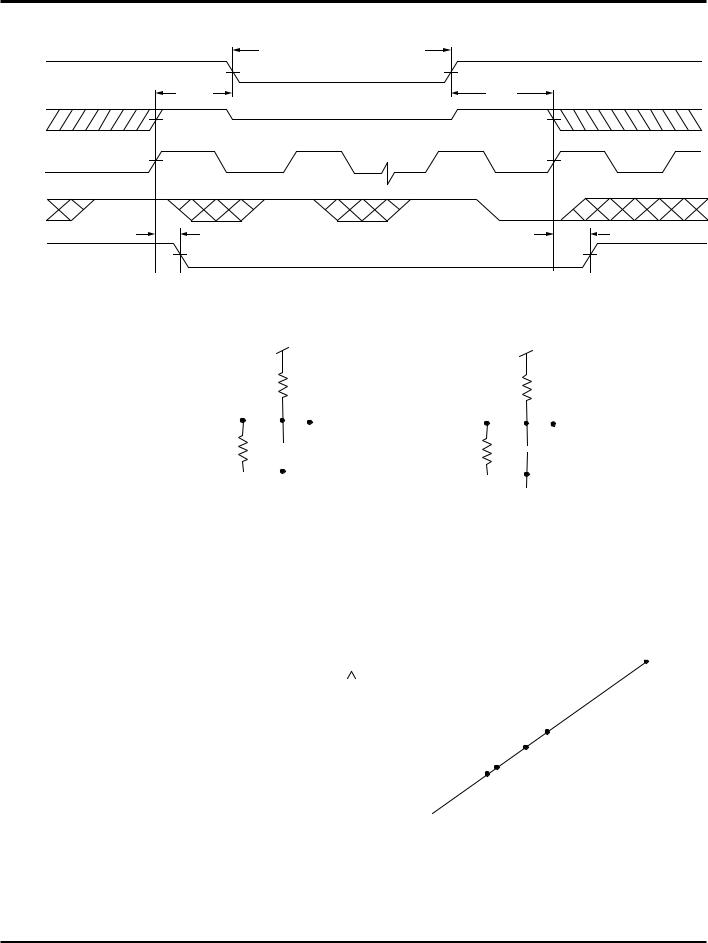
DATA RETENTION AND POWER DOWN/UP WAVEFORM (RANDOM AND SEQUENTIAL PORT) (1,2)
DATA RETENTION MODE
VCC |
4.5V |
VDR ³ 2V |
4.5V |
|
tCDR |
|
tR |
CE |
VIH |
VDR |
VIH |
|
|||
SCLK |
|
|
|
SCE |
|
|
|
|
tPD |
|
tPU |
ICC |
|
|
|
|
ISB |
|
3016 drw 04 |
NOTES : |
|
ISB |
|
|
|
|
|
1. SCE is synchronized to the sequential clock input. |
|
|
|
2. CMD > VCC - 0.2V. |
|
|
|
|
|
5V |
5V |
|
|
893Ω |
893Ω |
DATAOUT
|
|
|
|
|
|
|
|
|
|
|
|
DATAOUT |
|
|
|
|
|
|
|
|
|
|
|
|
|
347Ω |
|
|
|
|
|
30pF |
|
|
|
|
|
|
|
|
|||||||||
|
|
|
|
|
|
347Ω |
|
|
|
|
|
|
5pF |
|||||||||||
|
|
|
|
|
|
|
|
|
|
|
|
|
||||||||||||
|
|
|
||||||||||||||||||||||
|
|
|
|
|
|
|
|
|||||||||||||||||
|
|
|
|
|
|
|
|
|
|
|
|
|
|
|
|
|
|
|
|
|
|
|
|
|
|
|
|
|
|
|
|
|
|
|
|
|
|
|
|
|
|
|
|
|
|
|
|
|
|
|
|
|
|
|
|
|
|
|
|
|
|
|
|
|
|
|
|
|
|
|
|
|
|
|
|
|
|
|
|
|
|
|
|
|
|
|
|
|
|
|
|
|
|
|
|
|
|
|
|
|
|
|
|
|
|
|
|
|
|
|
|
|
|
|
|
|
|
|||||||
|
|
|
|
|
|
|
|
|
|
|
|
|
|
|
|
|
|
|
|
|
|
|
|
|
|
|
|
|
|
|
|
|
|
|
|
|
|
|
|
|
|
||||||||
|
|
|
|
|
|
|
|
|
|
|
|
|
|
|
|
|
|
|
|
|
|
|
|
|
|
|
|
|
|
|
3016 drw 05 |
|
|
|
|
|
|
3016 drw 06 |
|||||||||||
Figure 1. AC Output Test Load |
Figure 2. Output Test Load (for tCLZ, tBLZ, tOLZ, tCHZ, |
|||||||||||||||||||||||
|
|
|
|
|
|
|
|
|
|
|
|
|
tBHZ, tOHZ, tWHZ, tCKHZ, and tCKLZ) |
|||||||||||
Including scope and jig.
|
|
|
|
|
8 |
|
|
|
|
|
|
|
|
|
|
|
|
|
|
|
|
|
|
|
|
|
|
|
|
|
|
|
|
|
|
|
|
|
|
|
|
|
|
|
|
|
|
|
|
|
7 |
|
|
|
|
|
|
|
|
|
|
|
|
|
|
|
|
|
|
|
|
|
|
|
|
|
|
|
|
|
|
|
|
|
|
|
|
|
|
|
|
|
|
|
|
tAA/tCD/tEB |
6 |
|
|
|
|
|
|
|
|
|
|
|
|
|
|
|
|
|
|
|
|
|
|
|
|
|
|
|
|
|
|
|
|
|
|
|
|
|
|
||
|
|
|
|
5 |
|
|
|
|
|
|
|
|
|
|
|
|
|
|
|
|
|
|
|
|
|
|
(Typical, ns) |
4 |
|
|
|
|
|
|
|
|
|
|
|
|
|
|
|
|
|
|
|
|
|
|
|
|
|
|
|
|
|
|
|
|
|
|
10pF is the I/O |
|||||
|
|
|
|
|
|
|
|
|
|
|
|
|
|
|
|
|
||||||
|
|
|
|
|
3 |
|
|
|
|
|
|
|
|
|
|
|
|
|||||
AC TEST CONDITIONS |
|
|
|
|
|
|
|
|
|
|
|
|
|
|
|
|
capacitance of |
|||||
|
|
|
|
|
|
|
|
|
|
|
|
|||||||||||
|
|
|
|
2 |
|
|
|
|
|
|
|
|
|
|
|
|
this device, and |
|||||
|
|
|
|
|
|
|
|
|
|
|
|
|
|
|
|
|
30pF is the AC |
|||||
Input Pulse Levels |
GND to 3.0V |
|
|
|
|
|
|
|
|
|
|
|
|
|
|
|
||||||
|
1 |
|
|
|
|
|
|
|
|
|
|
|
|
Test Load |
||||||||
Input Rise/Fall Times |
3ns Max. |
|
|
|
|
|
|
|
|
|
|
|
|
|
|
|
capacitance. |
|||||
|
|
|
|
|
|
|
|
|
|
|
|
|
|
|
|
|||||||
|
-1 |
|
|
|
|
|
|
|
|
|
|
|
|
|
|
|
|
|
||||
Input Timing Reference Levels |
1.5V |
|
|
|
|
|
|
|
|
|
|
|
|
|
|
|
|
|
|
|
|
|
|
|
|
|
|
|
|
|
|
|
|
|
|
|
|
|
|
|
|||||
|
|
|
|
|
|
|
|
|
|
|
|
|
|
|
|
|||||||
|
20 40 |
60 |
80 100 120 140 160 180 200 |
|
||||||||||||||||||
Output Reference Levels |
1.5V |
|
|
|
-2 |
|
|
|||||||||||||||
|
|
|
|
|
|
|
|
|
CAPACITANCE (pF) |
3016 drw 07 |
||||||||||||
|
|
|
|
|
|
|
|
|||||||||||||||
AC Test Load |
Figures 1, 2, and 3 |
|
|
|
-3 |
|
|
|
|
|
|
|
|
|||||||||
|
|
|
|
|
|
|
|
|
|
|
|
|
|
|
|
|
|
|||||
|
|
|
|
|
|
|
|
|
|
|
|
|
|
|
|
|
||||||
|
|
|
|
|
|
|
|
|
|
|
|
|
|
|
|
|
|
|
|
|
||
|
3016 tbl 10 |
|
|
|
|
|
|
|
|
|
|
|
|
|
|
|
|
|
|
|||
Figure 3. Lumped Capacitance Load Typical Derating Curve
6.31 |
6 |
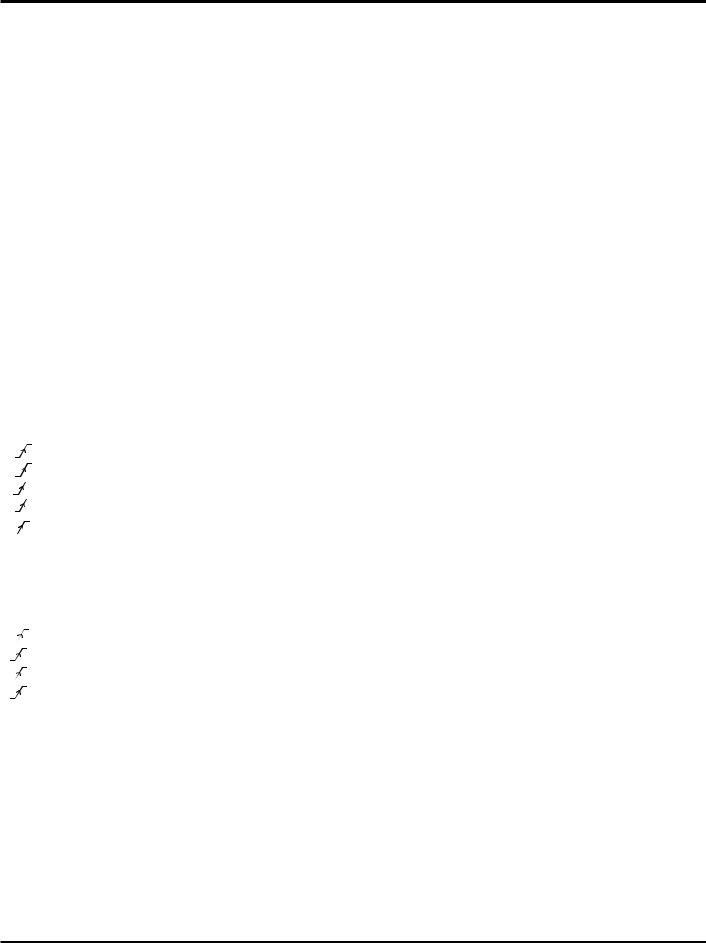
IDT70825S/L |
|
HIGH-SPEED 8K x 16 SEQUENTIAL ACCESS RANDOM ACCESS MEMORY |
MILITARY AND COMMERCIAL TEMPERATURE RANGES |
TRUTH TABLE I – RANDOM ACCESS READ AND WRITE(1,2)
|
|
Inputs/Outputs |
|
|
|
MODE |
|||
|
|
|
|
|
|
|
|
|
|
CE |
CMD |
R/W |
OE |
LB |
|
UB |
I/O0-I/O7 |
I/O8-I/O- |
|
|
|
|
|
|
|
|
|
|
|
L |
H |
H |
L |
L |
|
L |
DATAOUT |
DATAOUT |
Read both Bytes. |
|
|
|
|
|
|
|
|
|
|
L |
H |
H |
L |
L |
|
H |
DATAOUT |
High-Z |
Read lower Byte only. |
|
|
|
|
|
|
|
|
|
|
L |
H |
H |
L |
H |
|
L |
High-Z |
DATAOUT |
Read upper Byte only. |
|
|
|
|
|
|
|
|
|
|
L |
H |
L |
H(3) |
L |
|
L |
DATAIN |
DATAIN |
Write to both Bytes. |
L |
H |
L |
H(3) |
L |
|
H |
DATAIN |
High-Z |
Write to lower Byte only. |
L |
H |
L |
H(3) |
H |
|
L |
High-Z |
DATAIN |
Write to upper Byte only. |
H |
H |
X |
X |
X |
|
X |
High-Z |
High-Z |
Both Bytes deselected and powered down. |
|
|
|
|
|
|
|
|
|
|
L |
H |
H |
H |
X |
|
X |
High-Z |
High-Z |
Outputs disabled but not powered down. |
|
|
|
|
|
|
|
|
|
|
L |
H |
X |
X |
H |
|
H |
High-Z |
High-Z |
Both Bytes deselected but not powered down. |
|
|
|
|
|
|
|
|
|
|
H |
L |
L |
H(3) |
L(4) |
|
L(4) |
DATAIN |
DATAIN |
Write I/O0-I/O12 to the Buffer Command Register. |
H |
L |
H |
L |
L(4) |
|
L(4) |
DATAOUT |
DATAOUT |
Read contents of the Buffer Command Register via I/O0-I/O12. |
NOTES: |
|
|
|
|
|
|
|
3016 tbl 11 |
|
1.H = VIH, L = VIL, X = Don't Care, and High-Z = High-impedance.
2.RST, SCE, CNTEN, SR/W, SLD, SSTRT1, SSTRT2, SCLK, SI/O0-SI/O15, EOB1, EOB2, and SOE are unrelated to the random access port control and operation.
3.If OE = VIL during write, tWHZ must be added to the tWP or tCW write pulse width to allow the bus to float prior to being driven.
4.Byte operations to control register using UB and LB separately are also allowed.
TRUTH TABLE II – SEQUENTIAL READ(1,2,3,6,8)
|
|
Inputs/Outputs |
|
|
|
MODE |
||
SCLK |
SCE |
CNTEN |
SR/W |
EOB1 |
EOB2 |
SOE |
SI/O |
|
|
L |
L |
H |
LOW |
LAST |
L |
[EOB1] |
Counter Advanced Sequential Read with EOB1 reached. |
|
|
|
|
|
|
|
|
|
|
L |
H |
H |
LAST |
LAST |
L |
[EOB1 - 1] |
Non-Counter Advanced Sequential Read, without EOB1 reached. |
|
|
|
|
|
|
|
|
|
|
L |
L |
H |
LAST |
LOW |
L |
[EOB2] |
Counter Advanced Sequential Read with EOB2 reached. |
|
|
|
|
|
|
|
|
|
|
L |
H |
H |
LAST |
LAST |
L |
[EOB2 - 1] |
Non-Counter Advanced Sequential Read without EOB2 reached. |
|
L |
L |
H |
LOW |
LOW |
H |
HIGH-Z |
Counter Advanced Sequential Non-Read with EOB1 and EOB2 |
|
|
|
|
|
|
|
|
reached. |
|
|
|
|
|
|
|
|
3016 tbl 12 |
TRUTH TABLE III – SEQUENTIAL WRITE(1,2,3,4,5,6,7,8)
|
|
|
Inputs/Outputs |
|
|
MODE |
||
SCLK |
SCE |
CNTEN |
SR/W |
EOB1 |
EOB2 |
SOE |
SI/O |
|
|
|
|
|
|
|
|
|
|
|
L |
H |
L |
LAST |
LAST |
H |
SI/OIN |
Non-Counter Advanced Sequential Write, without EOB1 or EOB2 reached |
|
L |
L |
L |
LOW |
LOW |
H |
SI/OIN |
Counter Advanced Sequential Write with EOB1 and EOB2 reached. |
|
|
|
|
|
|
|
|
|
|
H |
H |
X |
LAST |
LAST |
X |
High-Z |
No Write or Read due to Sequential port Deselect. No counter advance. |
|
|
|
|
|
|
|
|
|
|
H |
L |
X |
NEXT |
NEXT |
X |
High-Z |
No Write or Read due to Sequential port Deselect. Conter does advance. |
|
|
|
|
|
|
|
|
|
NOTES: |
|
|
|
|
|
|
3016 tbl 13 |
|
1.H = VIH, L = VIL, X = Don't Care, and High-Z = High-impedance. LOW = VOL.
2.RST, SLD, SSTRT1, SSTRT2 are continuously HIGH during a sequential write access, other than pointer access operations.
3.CE, OE, R/W, CMD, LB, UB, and I/O0-I/O15 are unrelated to the sequential port control and operation except for CMD which must not be used concurrently with the sequential port operation (due to the counter and register control). CMD should be HIGH (CMD = VIH) during sequential port access.
4.SOE must be HIGH (SOE=VIH) prior to write conditions only if the previous cycle is a read cycle, since the data being written must be an input at the rising edge of the clock during the cycle in which SR/W = VIL.
5.SI/OIN refers to SI/O0-SI/O15 inputs.
6."LAST" refers to the previous value still being output, no change.
7.Termination of a write is done on the Low-to-High transition of SCLK if SR/W or SCE is High.
8.When CLKEN=Low, the address is incremented on the next rising edge before any operation takes place. See the diagrams called "Sequential Counter Enable Cycle after Reset, Read (and write) Cycle".
6.31 |
7 |
 Loading...