


IDT70261L20PF
Integrated Device Technology Inc IDT70261L20PF, IDT70261L25PF, IDT70261L35PF, IDT70261L55PF, IDT70261S20PF Datasheet
...
Integrated Device Technology, Inc.
HIGH-SPEED
16K x 16 DUAL-PORT
STATIC RAM WITH INTERRUPT
IDT70261S/L
FEATURES:
• True Dual-Ported memory cells which allow simultaneous access of the same memory location
• High-speed access
— Commercial: 20/25/35/55ns (max.)
• Low-power operation
— IDT70261S
Active: 750mW (typ.)
Standby: 5mW (typ.)
— IDT70261L
Active: 750mW (typ.)
Standby: 1mW (typ.)
• Separate upper-byte and lower-byte control for
multiplexed bus compatibility
• IDT70261 easily expands data bus width to 32 bits or
more using the Master/Slave select when cascading
more than one device
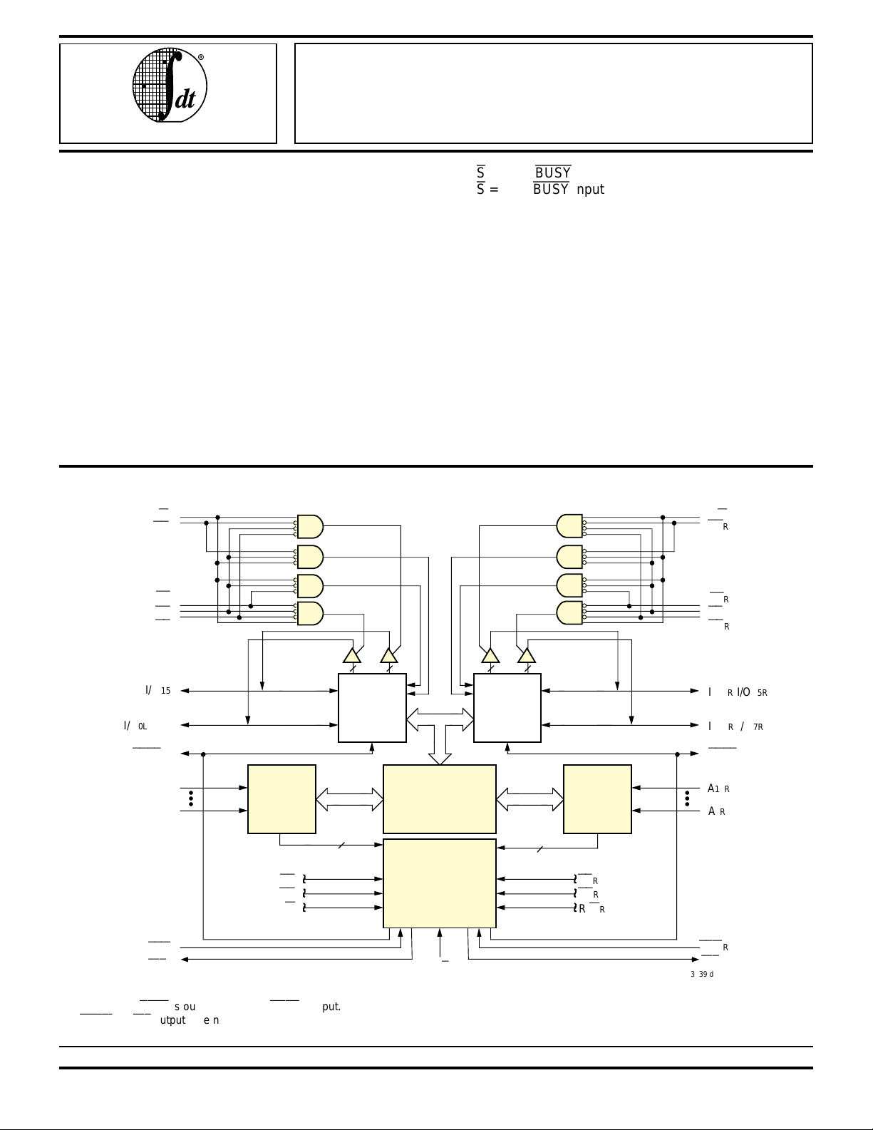
FUNCTIONAL BLOCK DIAGRAM
W
L
R/
UB
L
•M/S = H for
M/S = L for
BUSY
output flag on Master,
BUSY
input on Slave
• Busy and Interrupt Flags
• On-chip port arbitration logic
• Full on-chip hardware support of semaphore signaling
between ports
• Fully asynchronous operation from either port
• TTL-compatible, single 5V (±10%) power supply
• Available in 100-pin Thin Quad Plastic Flatpack
DESCRIPTION:
The IDT70261 is a high-speed 16K x 16 Dual-Port Static
RAM. The IDT70261 is designed to be used as a stand-alone
Dual-Port RAM or as a combination MASTER/SLAVE DualPort RAM for 32-bit-or-more word systems. Using the IDT
MASTER/SLAVE Dual-Port RAM approach in 32-bit or wider
memory system applications results in full-speed, error-free
W
R
R/
UB
R
LB
L
CE
L
OE
L
I/O8L-I/O
NOTES:
1. (MASTER):
2.
BUSY
and
The IDT logo is a registered trademark of Integrated Device Technology, Inc.
15L
I/O0L-I/O
7L
(1,2)
BUSY
L
A
13L
A
0L
SEM
L
(2)
INT
L
BUSY
is output; (SLAVE):
INT
outputs are non-tri-stated push-pull.
Address
Decoder
CE
OE
R/
W
BUSY
L
L
L
is input.
14
I/O
Control
MEMORY
ARRAY
ARBITRATION
INTERRUPT
SEMAPHORE
LOGIC
M/
S
I/O
Control
Address
Decoder
14
CE
R
OE
R
R/
W
R
LB
CE
OE
I/O8R-I/O
I/O0R-I/O
BUSY
A
13R
A
0R
SEM
INT
R
3039 drw 01
R
R
R
15R
7R
(1,2)
R
R
(2)
COMMERCIAL TEMPERATURE RANGE OCTOBER 1996
©1996 Integrated Device Technology, Inc. DSC 3039/3
For latest information contact IDT’s web site at www.idt.com or fax-on-demand at 408-492-8391.
6.18
1
IDT70261S/L
HIGH-SPEED 16K x 16 DUAL-PORT STATIC RAM WITH INTERRUPT COMMERCIAL TEMPERATURE RANGE
operation without the need for additional discrete logic.
This device provides two independent ports with separate
control, address, and I/O pins that permit independent,
asynchronous access for reads or writes to any location in
memory. An automatic power down feature controlled by
Index
N/C
N/C
N/C
N/C
I/O
I/O
I/O
I/O
GND
I/O
I/O
V
GND
I/O
I/O
I/O
V
I/O
I/O
I/O
I/O
N/C
N/C
N/C
N/C
(1,2)
9L
8L
7L
6L
5L
4L
I/O
I/O
I/O
3L
I/O
I/O
I/O
I/O
100 9998 97 96 95 94 93 92 91 90 89 88 87 86 85 84 83 82 81 80 79 78 7776
1
2
3
4
10L
5
11L
6
12L
7
13L
8
9
14L
10
15L
11
CC
12
13
0R
14
1R
15
2R
16
CC
17
3R
18
4R
19
5R
20
6R
21
22
23
24
25
26 27 28 29 30 31 32 33 34 35 36 37 38 39 40 41 42 43 44 45 46 47 48 49 50
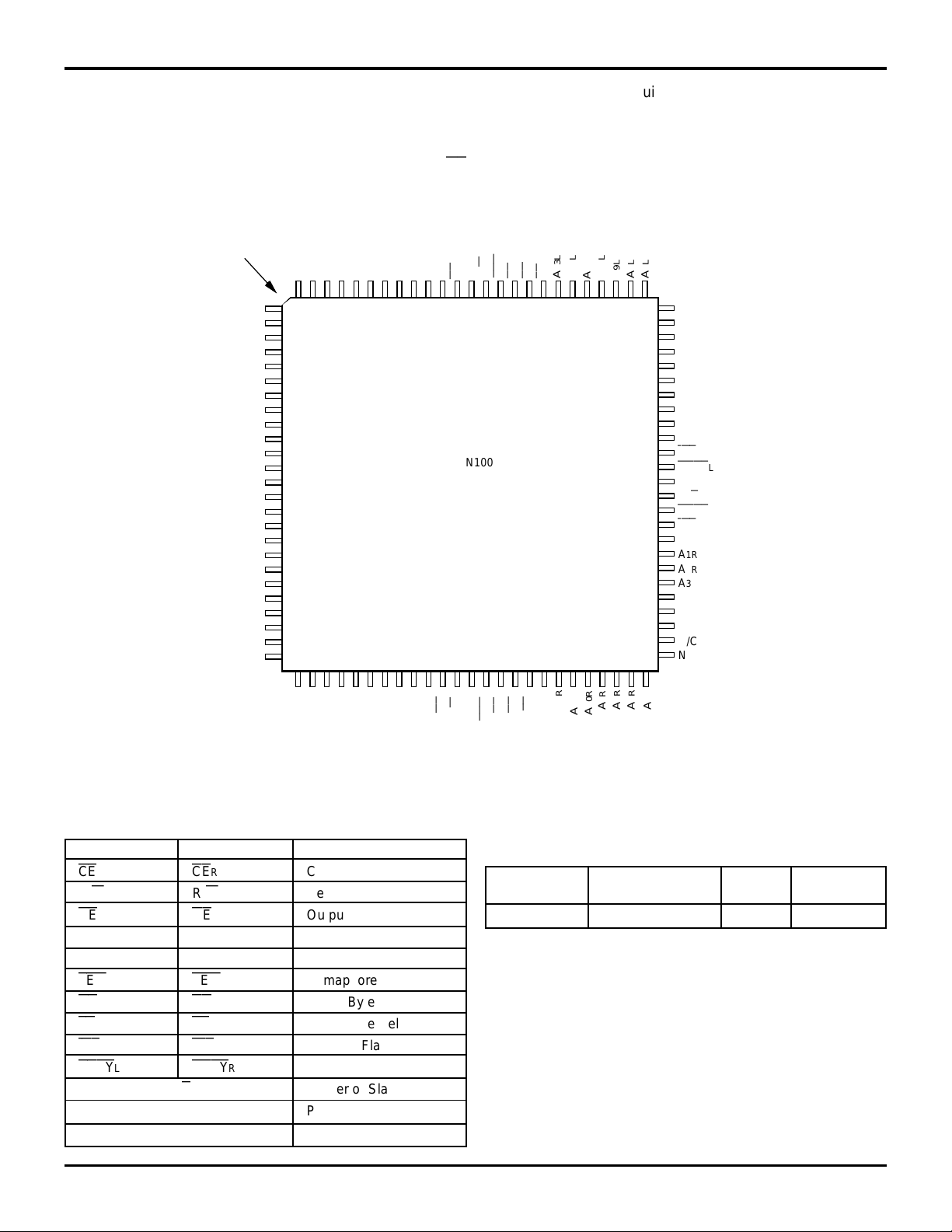
PIN CONFIGURATIONS
2L
I/O
GND
1L
I/O
CE
0L
I/O
TOP VIEW
permits the on-chip circuitry of each port to enter a very low
standby power mode.
Fabricated using IDT’s CMOS high-performance technol-
ogy, these devices typically operate on only 750mW of power.
The IDT70261 is packaged in a 100-pin TQFP.
L
L
L
CC
V
L
SEM
(3)
CE
UB
L
LB
13L
A
12L
A
11L
A
10L
A
9L
8L
7L
A
A
A
N/C
75
N/C
74
N/C
73
72
6L
A
A
71
5L
70
A
4L
69
A
3L
68
A
2L
67
A
1L
66
A
0L
INT
BUSY
GND
M/
S
BUSY
INT
A
0R
A
1R
A
2R
A
3R
A
4R
A
5R
N/C
N/C
N/C
L
L
R
R
65
64
63
62
61
60
59
58
57
56
55
54
53
52
51
W
R/
L
OE
IDT70261
PN100-1
100-PIN
TQFP
7R
8R
9R
11R
12R
13R
I/O
I/O
I/O
10R
I/O
I/O
I/O
I/O
14R
I/O
NOTES:
CC pins must be connected to power supply.
1. All V
2. All GND pins must be connected to ground supply.
3. This text does not indicate orientation of the actual part-marking.
PIN NAMES
Left Port Right Port Names
CE
L
R/
W
L R/WR Read/Write Enable
OE
L
A
0L – A13L A0R – A13R Address
I/O
0L – I/O15L I/O0R – I/O15R Data Input/Output
SEM
L
UB
L
LB
L
INT
L
BUSY
L
CE
R Chip Enable
OE
R Output Enable
SEM
R Semaphore Enable
UB
R Upper Byte Select
LB
R Lower Byte Select
INT
R Interrupt Flag
BUSY
R Busy Flag
M/
S
V
CC Power
Master or Slave Select
GND Ground
15R
GND
I/O
3039 tbl 01
R
SEM
R
CE
R
UB
R
LB
13R
A
12R
A
11R
A
10R
A
3039 drw 02
8R
7R
6R
9R
A
A
A
A
R
OE
R
W
GND
R/
RECOMMENDED OPERATING
TEMPERATURE AND SUPPLY VOLTAGE
Ambient
Grade Temperature GND V
Commercial 0°C to +70°C 0V 5.0V ± 10%
CC
3039 tbl 02
6.18 2
IDT70261S/L
HIGH-SPEED 16K x 16 DUAL-PORT STATIC RAM WITH INTERRUPT COMMERCIAL TEMPERATURE RANGE
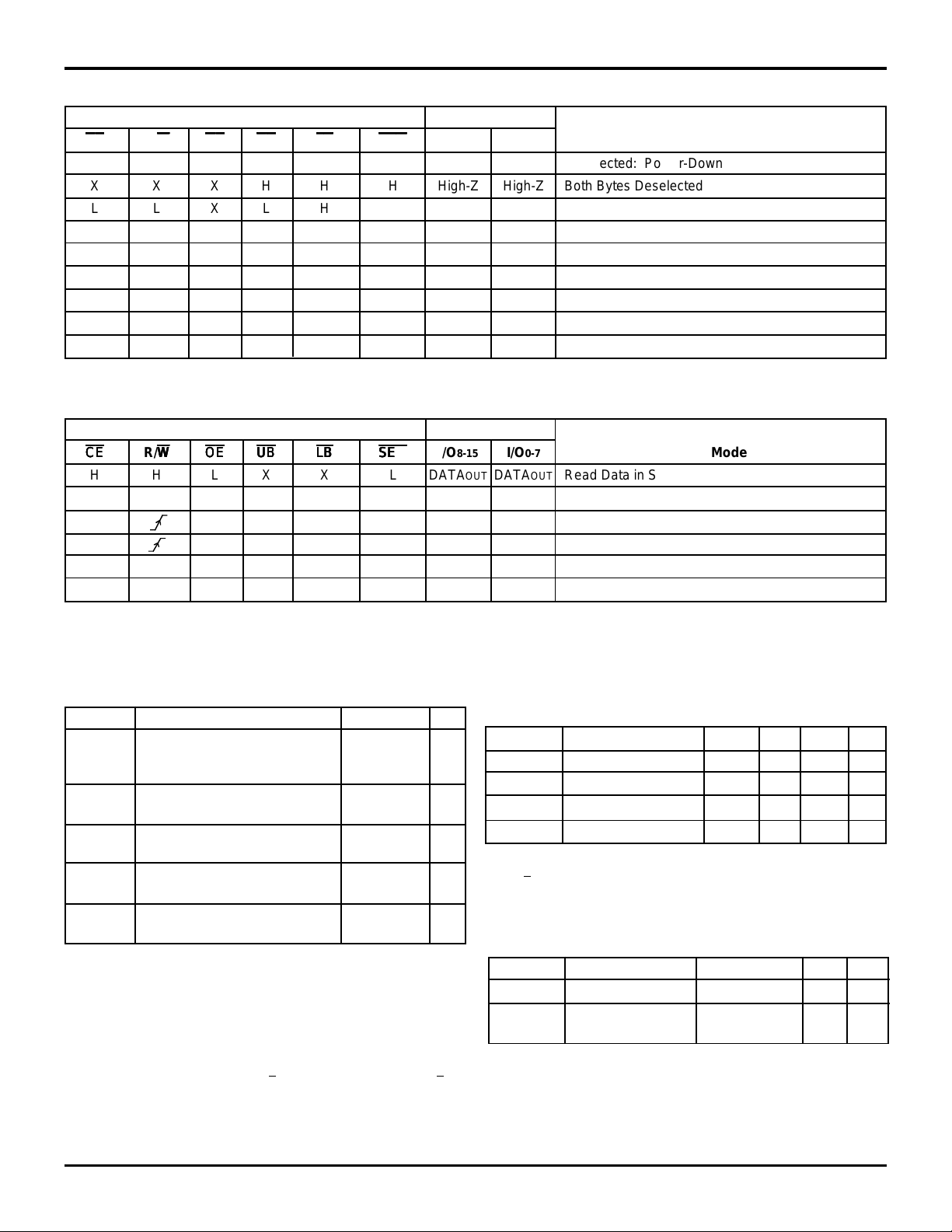
TRUTH TABLE I – NON-CONTENTION READ/WRITE CONTROL
(1)
Inputs
CECE
CE
CECE
R/
WW
W
WW
OEOE
OE
OEOE
UBUB
UB
UBUB
LBLB
LB
LBLB
SEMSEM
SEM
SEMSEM
H X X X X H High-Z High-Z Deselected: Power-Down
X X X H H H High-Z High-Z Both Bytes Deselected
L L X L H H DATA
L L X H L H High-Z DATA
L L X L L H DATA
L H L L H H DATA
L H L H L H High-Z DATA
L H L L L H DATA
X X H X X X High-Z High-Z Outputs Disabled
NOTE: 3039 tbl 03
1. A0L — A13L ≠ A0R — A13R.
TRUTH TABLE II – SEMAPHORE READ/WRITE CONTROL
Inputs Outputs
CECE
CE
CECE
H H L X X L DATA
X H L H H L DATA
H X X X L DATA
X
L X X L X L — — Not Allowed
L X X X L L — — Not Allowed
NOTE:
1. There are eight semaphore flags written to via I/O
R/
WW
W
WW
OEOE
OE
OEOE
UBUB
UB
UBUB
LBLB
LB
LBLB
SEMSEM
SEM
SEMSEM
X H H L DATAIN DATAIN Write I/O0 into Semaphore Flag
0 and read from all I/O's(I/O0 - I/O15). These eight semaphores are addressed by A0 - A2.
Outputs
8-15 I/O0-7 Mode
I/O
IN High-Z Write to Upper Byte Only
IN Write to Lower Byte Only
IN DATAIN Write to Both Bytes
OUT High-Z Read Upper Byte Only
OUT Read Lower Byte Only
OUT DATAOUT Read Both Bytes
(1)
8-15 I/O0-7 Mode
I/O
OUT DATAOUT Read Data in Semaphore Flag
OUT DATAOUT Read Data in Semaphore Flag
IN DATAIN Write I/O0 into Semaphore Flag
3039 tbl 04
ABSOLUTE MAXIMUM RATINGS
(1)
Symbol Rating Commercial Unit
(2)
V
TERM
Terminal Voltage –0.5 to +7.0 V
with Respect
to GND
T
A Operating 0 to +70 °C
Temperature
T
BIAS Temperature –55 to +125 °C
Under Bias
STG Storage –55 to +125 °C
T
Temperature
I
OUT DC Output 50 mA
Current
NOTES: 3039 tbl 05
1. Stresses greater than those listed under ABSOLUTE MAXIMUM
RATINGS may cause permanent damage to the device. This is a stress
rating only and functional operation of the device at these or any other
conditions above those indicated in the operational sections of this
specification is not implied. Exposure to absolute maximum rating
conditions for extended periods may affect reliability.
TERM must not exceed Vcc + 0.5V for more than 25% of the cycle time
2. V
or 10ns maximum, and is limited to
+ 0.5V.
< 20mA for the period of VTERM > Vcc
RECOMMENDED DC OPERATING
CONDITIONS
Symbol Parameter Min. Typ. Max. Unit
CC Supply Voltage 4.5 5.0 5.5 V
V
GND Supply Voltage 0 0 0 V
(2)
Max. Unit
(2)
V
IH Input High Voltage 2.2 — 6.0
V
V
IL Input Low Voltage –0.5
(1)
— 0.8 V
NOTES: 3039 tbl 06
1. VIL > -1.5V for pulse width less than 10ns.
TERM must not exceed Vcc + 0.5V.
2. V
CAPACITANCE
(1)
(TA = +25°C, f = 1.0MHz)TQFP ONLY
Symbol Parameter Conditions
IN Input Capacitance VIN = 3dV 9 pF
C
OUT Output VOUT = 3dV 10 pF
C
Capacitance
NOTES: 3039 tbl 07
1. This parameter is determined by device characterization but is not
production tested.
2. 3dV represents the interpolated capacitance when the input and output
signals switch from 0V to 3V or from 3V to 0V.
6.18 3
IDT70261S/L
HIGH-SPEED 16K x 16 DUAL-PORT STATIC RAM WITH INTERRUPT COMMERCIAL TEMPERATURE RANGE
DC ELECTRICAL CHARACTERISTICS OVER THE
OPERATING TEMPERATURE AND SUPPLY VOLTAGE RANGE
Symbol Parameter Test Conditions Min. Max. Min. Max. Unit
LI| Input Leakage Current
|I
LO| Output Leakage Current
|I
OL Output Low Voltage IOL = 4mA — 0.4 — 0.4 V
V
OH Output High Voltage IOH = -4mA 2.4 — 2.4 — V
V
NOTE: 3039 tbl 08
1. At Vcc < 2.0V, input leakages are undefined.
(1)
VCC = 5.5V, VIN = 0V to VCC —10—5µA
CE
= VIH, VOUT = 0V to VCC —10—5µA
(VCC = 5.0V ± 10%)
IDT70261S IDT70261L
DC ELECTRICAL CHARACTERISTICS OVER THE
OPERATING TEMPERATURE AND SUPPLY VOLTAGE RANGE
Test
Symbol Parameter Condition Version Typ.
CC Dynamic Operating
I
Current
(Both Ports Active) f = f
ISB1 Standby Current
(Both Ports — TTL
Level Inputs) f = f
ISB2 Standby Current
(One Port — TTL Active Port Outputs Open, L 115 180 105 170
Level Inputs) f = f
ISB3 Full Standby Current Both Ports
(Both Ports — All
CMOS Level Inputs) V
SB4 Full Standby Current
I
(One Port — All
CMOS Level Inputs)
CE
= VIL, Outputs Open COM’L. S 180 315 170 305 mA
SEM
= V
IH L 180 275 170 265
(3)
MAX
CE
R = CEL = VIH COM’L. S 30 85 25 85 mA
SEM
R =
SEM
L = VIH L 30602560
(3)
MAX
CE
"A" = VIL and CE"B" = VIH
(3)
MAX
SEM
R =
SEM
L = VIH
CE
L and COM’L. S 1.0 15 1.0 15 mA
CE
R > VCC - 0.2V L 0.2 5 0.2 5
IN > VCC - 0.2V or
V
IN < 0.2V, f = 0
SEM
R =
CE
"A" < 0.2V and COM’L. S 110 185 100 170 mA
CE
"B" > VCC - 0.2V
R =
SEM
V
IN > VCC - 0.2V or
IN < 0.2V
V
Active Port Outputs Open,
(3)
f = f
MAX
SEM
L > VCC - 0.2V
SEM
L > VCC - 0.2V
(4)
(5)
(5)
(1)
(VCC = 5.0V ± 10%)
COM’L. S 115 210 105 200 mA
L 110 160 100 145
70261X20 70261X25
(2)
Max. Typ.
(2)
Max. Unit
NOTES: 3039 tbl 09
1. "X" in part numbers indicates power rating (S or L).
CC = 5V, TA = +25°C, and are not production tested. ICCDC = 120mA (Typ.)
2. V
3. At f = f
4. f = 0 means no address or control lines change.
5. Port "A" may be either left or right port. Port "B" is the opposite from port "A".
MAX, address and control lines (except Output Enable) are cycling at the maximum frequency read cycle of 1 / tRC, and using “AC Test Conditions”
of input levels of GND to 3V.
6.18 4
IDT70261S/L
HIGH-SPEED 16K x 16 DUAL-PORT STATIC RAM WITH INTERRUPT COMMERCIAL TEMPERATURE RANGE
DC ELECTRICAL CHARACTERISTICS OVER THE
OPERATING TEMPERATURE AND SUPPLY VOLTAGE RANGE
Test
Symbol Parameter Condition Version Typ.
CC Dynamic Operating
I
Current
(Both Ports Active) f = f
ISB1 Standby Current
(Both Ports — TTL
Level Inputs) f = f
ISB2 Standby Current
(One Port — TTL Active Port Outputs Open, L 95 155 85 135
Level Inputs) f = f
ISB3 Full Standby Current Both Ports
(Both Ports — All
CMOS Level Inputs) V
SB4 Full Standby Current
I
(One Port — All
CMOS Level Inputs)
NOTES: 3039 tbl 10
1. "X" in part numbers indicates power rating (S or L).
CC = 5V, TA = +25°C, and are not production tested. ICCDC = 120mA (Typ.)
2. V
3. At f = f
4. f = 0 means no address or control lines change.
5. Port "A" may be either left or right port. Port "B" is the opposite from port "A".
MAX, address and control lines (except Output Enable) are cycling at the maximum frequency read cycle of 1/ tRC, and using
“AC Test Conditions” of input levels of GND to 3V.
CE
= VIL, Outputs Open COM’L. S 160 295 150 270 mA
SEM
= V
IH L 160 255 150 230
(3)
MAX
CE
R = CEL = VIH COM’L. S 20 85 13 85 mA
SEM
R =
SEM
L = VIH L 20601360
(3)
MAX
CE
"A" = VIL and CE"B" = VIH
(3)
MAX
SEM
R =
SEM
L = VIH
CE
L and COM’L. S 1.0 15 1.0 15 mA
CE
R > VCC - 0.2V L 0.2 5 0.2 5
IN > VCC - 0.2V or
V
IN < 0.2V, f = 0
SEM
R =
CE
"A" < 0.2V and COM’L. S 90 160 90 135 mA
CE
"B" > VCC - 0.2V
R =
SEM
V
IN > VC 265
IN < 0.2V
V
Active Port Outputs Open,
(3)
f = f
MAX
SEM
L > VCC - 0.2V
SEM
L > VCC - 0.2V
(4)
(5)
(5)
(1)
(VCC = 5.0V ± 10%)
70261X35 70261X55
(2)
Max. Typ.
(2)
Max. Unit
COM’L. S 95 185 85 165 mA
L 90 135 80 110
6.18 5
IDT70261S/L
HIGH-SPEED 16K x 16 DUAL-PORT STATIC RAM WITH INTERRUPT COMMERCIAL TEMPERATURE RANGE
AC TEST CONDITIONS
5V
Input Pulse Levels GND to 3.0V
Input Rise/Fall Times 5ns Max.
Input Timing Reference Levels 1.5V
Output Reference Levels 1.5V
DATA
OUT
BUSY
INT
893Ω
30pF347Ω
DATA
OUT
Output Load Figures 1 and 2
3039 tbl 11
2939 drw 03
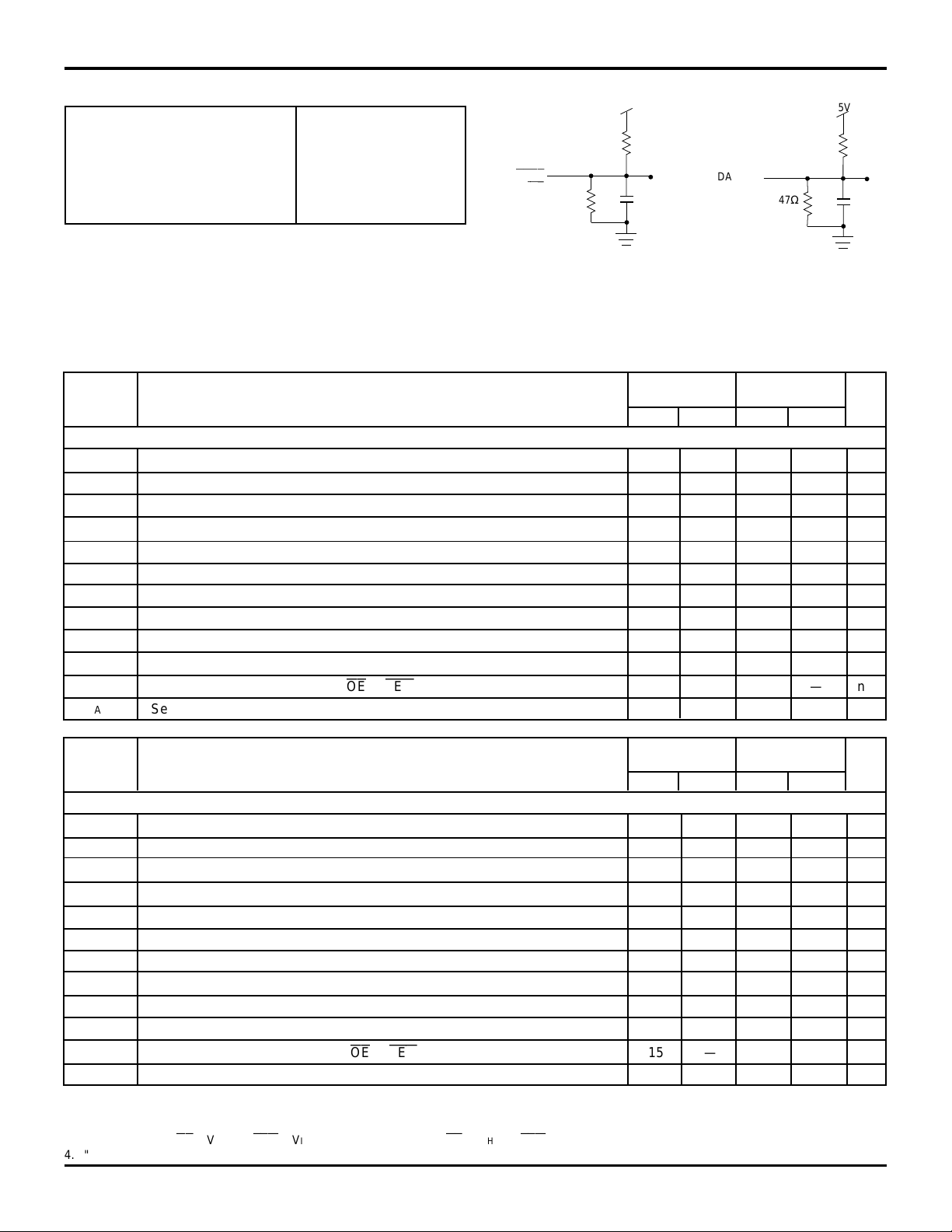
Figure 1. AC Output Test Load Figure 2. Output Test Load
(for t
Including scope and jig.
LZ, tHZ, tWZ, tOW)
AC ELECTRICAL CHARACTERISTICS OVER THE
OPERATING TEMPERATURE AND SUPPLY VOLTAGE RANGE
Symbol Parameter Min. Max. Min. Max. Unit
READ CYCLE
RC Read Cycle Time 20 — 25 — ns
t
AA Address Access Time — 20 — 25 ns
t
(1, 2)
(1, 2)
(3)
(3)
(2)
OE
(2)
or
SEM
)10—12—ns
ACE Chip Enable Access Time
t
ABE Byte Enable Access Time
t
AOE Output Enable Access Time — 12 — 13 ns
t
OH Output Hold from Address Change 3 — 3 — ns
t
LZ Output Low-Z Time
t
HZ Output High-Z Time
t
PU Chip Enable to Power Up Time
t
PD Chip Disable to Power Down Time
t
SOP Semaphore Flag Update Pulse (
t
SAA Semaphore Address Access Time — 20 — 25 ns
t
(4)
IDT70261X20 IDT70261X25
—20—25ns
—20—25ns
3—3—ns
—12—15ns
0—0—ns
—20—25ns
5V
893Ω
5pF347Ω
2939 drw 04
IDT70261X35 IDT70261X55
Symbol Parameter Min. Max. Min. Max. Unit
READ CYCLE
RC Read Cycle Time 35 — 55 — ns
t
AA Address Access Time — 35 — 55 ns
t
ACE Chip Enable Access Time
t
ABE Byte Enable Access Time
t
AOE Output Enable Access Time — 20 — 30 ns
t
OH Output Hold from Address Change 3 — 3 — ns
t
LZ Output Low-Z Time
t
HZ Output High-Z Time
t
PU Chip Enable to Power Up Time
t
PD Chip Disable to Power Down Time
t
SOP Semaphore Flag Update Pulse (
t
SAA Semaphore Address Access Time — 35 — 55 ns
t
NOTES:
1. Transition is measured ±200mV from Low or High-impedance voltage with Output Test Load (Figure 2).
2. This parameter is guaranteed by device characterization, but is not production tested.
3. To access RAM, CE = V
4. "X" in part numbers indicates power rating (S or L).
IL and
SEM
(3)
(3)
(1, 2)
(1, 2)
(2)
(2)
OE
or
SEM
)15—15—ns
= VIH. To access semaphore, CE = VIH and
6.18 6
SEM
—35—55ns
—35—55ns
3—3—ns
—15—25ns
0—0—ns
—35—50ns
= VIL.
3039 tbl 12
 Loading...