


IDT70V07L25G
Integrated Device Technology Inc IDT70V07L25G, IDT70V07L25J, IDT70V07L25PF, IDT70V07L35J, IDT70V07L35PF Datasheet
...
Integrated Device Technology, Inc.
COMMERCIAL TEMPERATURE RANGE OCTOBER 1996
©1996 Integrated Device Technology, Inc. DSC-2943/3
IDT70V07S/L
HIGH-SPEED 3.3V
32K x 8 DUAL-PORT
STATIC RAM
FEATURES:
• True Dual-Ported memory cells which allow simulta-
neous access of the same memory location
• High-speed access
— Commercial: 25/35/55ns (max.)
• Low-power operation
— IDT70V07S
Active: 450mW (typ.)
Standby: 5mW (typ.)
— IDT70V07L
Active: 450mW (typ.)
Standby: 5mW (typ.)
• IDT70V07 easily expands data bus width to 16 bits or
more using the Master/Slave select when cascading
more than one device
•M/
S
= H for
BUSY
output flag on Master
M/
S
= L for
BUSY
input on Slave
• Busy and Interrupt Flags
• On-chip port arbitration logic
• Full on-chip hardware support of semaphore signaling
between ports
• Fully asynchronous operation from either port
• Devices are capable of withstanding greater than 2001V
electrostatic discharge
• LVTTL-compatible, single 3.3V (±0.3V) power supply
• Available in 68-pin PGA, 68-pin PLCC, and a 64-pin
TQFP
DESCRIPTION:
The IDT70V07 is a high-speed 32K x 8 Dual-Port Static
RAM. The IDT70V07 is designed to be used as a stand-alone
Dual-Port RAM or as a combination MASTER/SLAVE Dual-
Port RAM for 16-bit-or-more word systems. Using the IDT
MASTER/SLAVE Dual-Port RAM approach in 16-bit or wider
memory system applications results in full-speed, error-free
operation without the need for additional discrete logic.
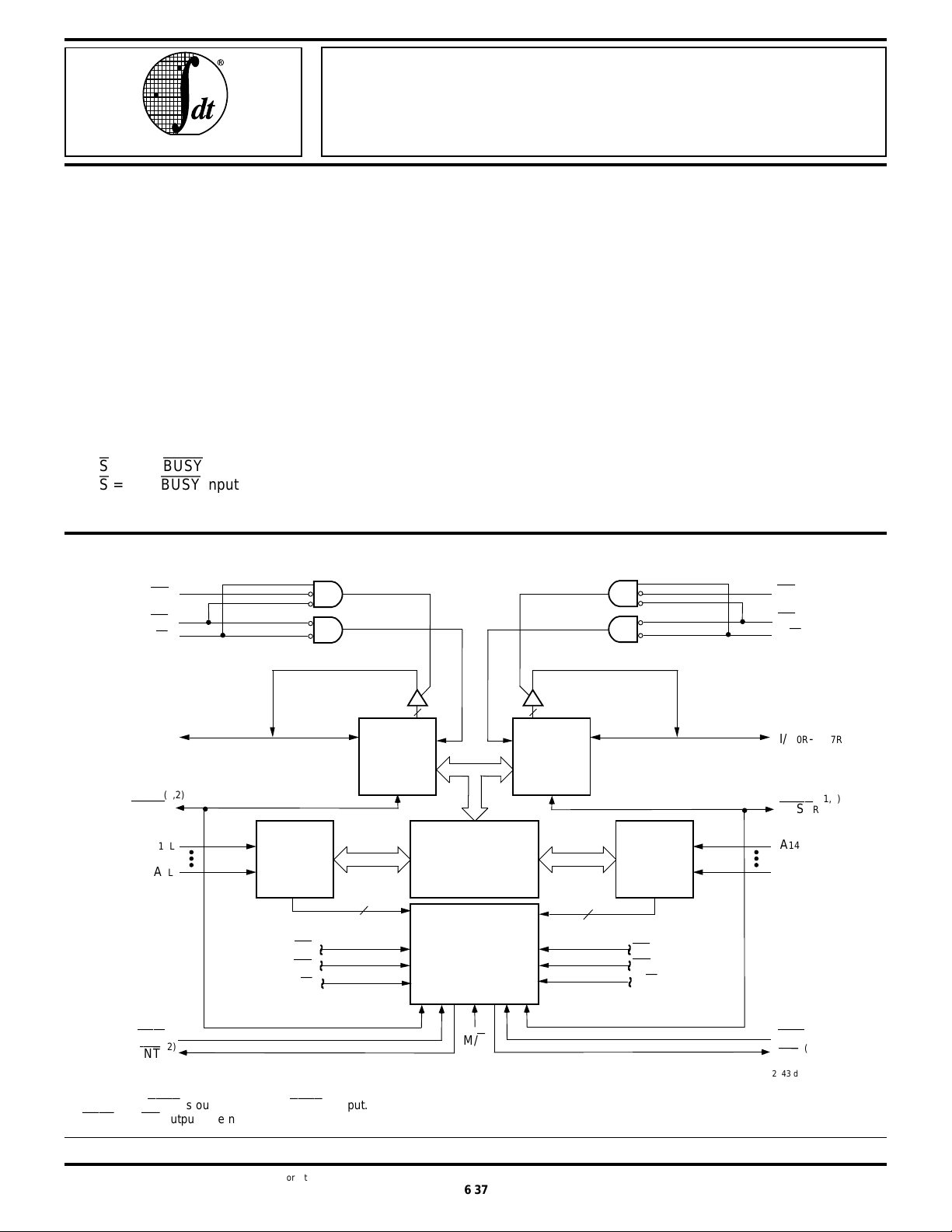
FUNCTIONAL BLOCK DIAGRAM
NOTES:
1. (MASTER):
BUSY
is output; (SLAVE):
BUSY
is input.
2.
BUSY
and
INT
outputs are non-tri-stated push-pull.
1
I/O
Control
Address
Decoder
MEMORY
ARRAY
ARBITRATION
INTERRUPT
SEMAPHORE
LOGIC
Address
Decoder
I/O
Control
R/
W
L
CE
L
OE
L
BUSY
L
A
14L
A
0L
2943 drw 01
I/O
0L
- I/O
7L
CE
L
OE
L
R/
W
L
SEM
L
INT
L
M/
S
BUSY
R
I/O
0R
-I/O
7R
A
14R
A
0R
SEM
R
INT
R
CE
R
OE
R
(2)
(1,2)
(1,2)
(2)
R/
W
R
CE
R
OE
R
R/
W
R
15
15
6.37
For latest information contact IDT’s web site at www.idt.com or fax-on-demand at 408-492-8391.
6.37 2
IDT70V07S/L
HIGH-SPEED 3.3V 32K x 8 DUAL-PORT STATIC RAM COMMERCIAL TEMPERATURE RANGE
This device provides two independent ports with separate
control, address, and I/O pins that permit independent,
asynchronous access for reads or writes to any location in
memory. An automatic power down feature controlled by
CE
permits the on-chip circuitry of each port to enter a very low
standby power mode.
Fabricated using IDT’s CMOS high-performance technol-
ogy, these devices typically operate on only 450mW of power.
The IDT70V07 is packaged in a ceramic 68-pin PGA, a 68-
pin PLCC, and a 80-pin thin plastic quad flatpack (TQFP).
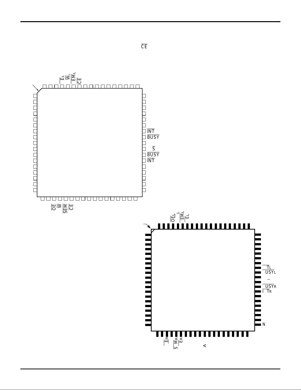
PIN CONFIGURATIONS
(1,2)
2943 drw 02
12
13
14
15
16
17
18
INDEX
19
20
21
22
98765432168676665
27 28 29 30 31 32 33 34 35 36 37 38 39
VCC
VCC
I/O1R
I/O2R
I/O3R
I/O4R
INT
L
GND
A
4L
A3L
A2L
A1L
A0L
A3R
A0R
A1R
A2R
I/O2L
A5L
11
10
M/
S
23
24
25
26
40 41 42 43
58
57
56
55
54
53
52
51
50
49
48
59
60
47
46
45
44
64 63 62 61
I/O3L
GND
I/O
0R
VCC
A4R
BUSY
L
GND
BUSY
R
INT
R
A12R
I/O7R
N/C
GND
OE
R
R/
W
R
SEM
R
CE
R
CE
L
N/C
I/O
0L
I/O1L
IDT70V07
J68-1
PLCC
TOP
VIEW
(3)
I/O
4L
I/O5L
I/O6L
I/O7L
I/O5R
I/O6R
A12L
A11R
A10R
A9R
A8R
A7R
A6R
A5R
A11L
A10L
A9L
A8L
A7L
A6L
A13R
A13L
A14L
A14R
R/
W
L
OE
L
SEM
L
INDEX
I/O
2L
V
CC
GND
GND
A
4R
BUSY
L
BUSY
R
GND
M/
S
OE
L
I/O
1L
R/
W
L
CE
L
SEM
L
V
CC
OE
R
CE
R
R/
W
R
SEM
R
A
12R
GND
I/O
3L
I/O
4L
I/O
5L
I/O
6L
I/O
7L
I/O
0R
I/O
1R
I/O
2R
V
CC
I/O
3R
I/O
4R
I/O
5R
I/O
7R
A
11R
A
10R
A
9R
A
8R
A
7R
A
6R
A
5R
A
3R
A
2R
A
1R
A
0R
A
0L
A
1L
A
2L
A
3L
A
4L
A
6L
A
7L
A
8L
A
9L
A
10L
A
11L
A
12L
I/O
0L
2943 drw 03
A
13R
A
13L
70V07
PN80-1
TQFP
TOP
VIEW
(3)
8
9
10
11
12
13
14
15
16
1
2
3
4
5
6
7
46
45
44
43
42
41
56
55
54
53
52
51
50
47
48
49
32
31
30
29
28
27
26
25
24
23
22
21
63
62
61
64
33
34
35
36
37
38
39
40
65
66
67
68
69
70
71
72
73
74
75
76
77
78
79
80
N/C
N/C
A
14L
N/C
N/C
N/C
N/C
A
14R
N/C
N/C
17
18
19
20
57
58
59
60
A
5L
N/C
INT
L
INT
R
N/C
N/C
N/C
I/O
6R
N/C
N/C
NOTES:
1. All Vcc pins must be connected to the power supply.
2. All GND pins must be connected to the ground supply.
3. This text does not indicate the actual part marking.
IDT70V07S/L
HIGH-SPEED 3.3V 32K x 8 DUAL-PORT STATIC RAM COMMERCIAL TEMPERATURE RANGE
6.37 3
NOTES:
1. All V
CC pins must be connected to power supply.
2. All GND pins must be connected to ground supply.
3. This text does not indicate orientation of the actual part-marking.
2943 tbl 01
Left Port Right Port Names
CE
L
CE
R Chip Enable
R/
W
L R/
W
R Read/Write Enable
OE
L
OE
R Output Enable
A
0L – A14L A0R – A14R Address
I/O
0L – I/O7L I/O0R – I/O7R Data Input/Output
SEM
L
SEM
R Semaphore Enable
INT
L
INT
R Interrupt Flag
BUSY
L
BUSY
R Busy Flag
M/
S
Master or Slave Select
V
CC Power
GND Ground
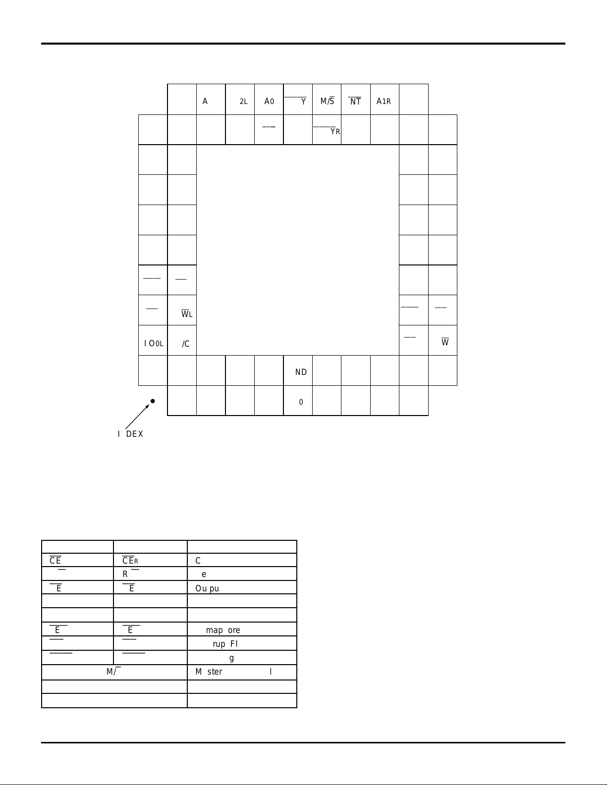
PIN NAMES
2943 drw 04
51 50 48 46 44 42 40 38 36
53
55
57
59
61
63
65
67
68
66
13579
11 13 15
20
22
24
26
28
30
32
35
IDT70V07
G68-1
68-PIN PGA
TOP VIEW
ABCDEFGHJ
K
L
47 45 43 41 34
21
23
25
27
29
31
33
2 4 6 8 10 12 14 16
18 19
17
56
58
60
62
64
11
10
09
08
07
06
05
04
03
02
01
52
54
49 39 37
A
5L
INT
L
SEM
L
CE
L
V
CC
OE
L
R/
W
L
I/O
0L
N/C
GND GND
I/O
0R
V
CC
N/C
OE
R
R/
W
R
SEM
R
CE
R
GND
BUSY
R
BUSY
L
M/
S
INT
R
GND
A
1R
INDEX
A
4L
A
2L
A
0L
A
3R
A
2R
A
4R
A
5R
A
7R
A
6R
A
9R
A
8R
A
11R
A
10R
A
12R
A
0R
A
7L
A
6L
A
3L
A
1L
A
9L
A
8L
A
11L
A
10L
A
12L
V
CC
I/O
2R
I/O
3R
I/O
5R
I/O
6R
I/O
1R
I/O
4R
I/O
7R
I/O
1L
I/O
2L
I/O
4L
I/O
7L
I/O
3L
I/O
5L
I/O
6L
A
13R
A
13L
A
14R
A
14L
(3)
PIN CONFIGURATIONS (CONT'D)
(1,2)
6.37 4
IDT70V07S/L
HIGH-SPEED 3.3V 32K x 8 DUAL-PORT STATIC RAM COMMERCIAL TEMPERATURE RANGE
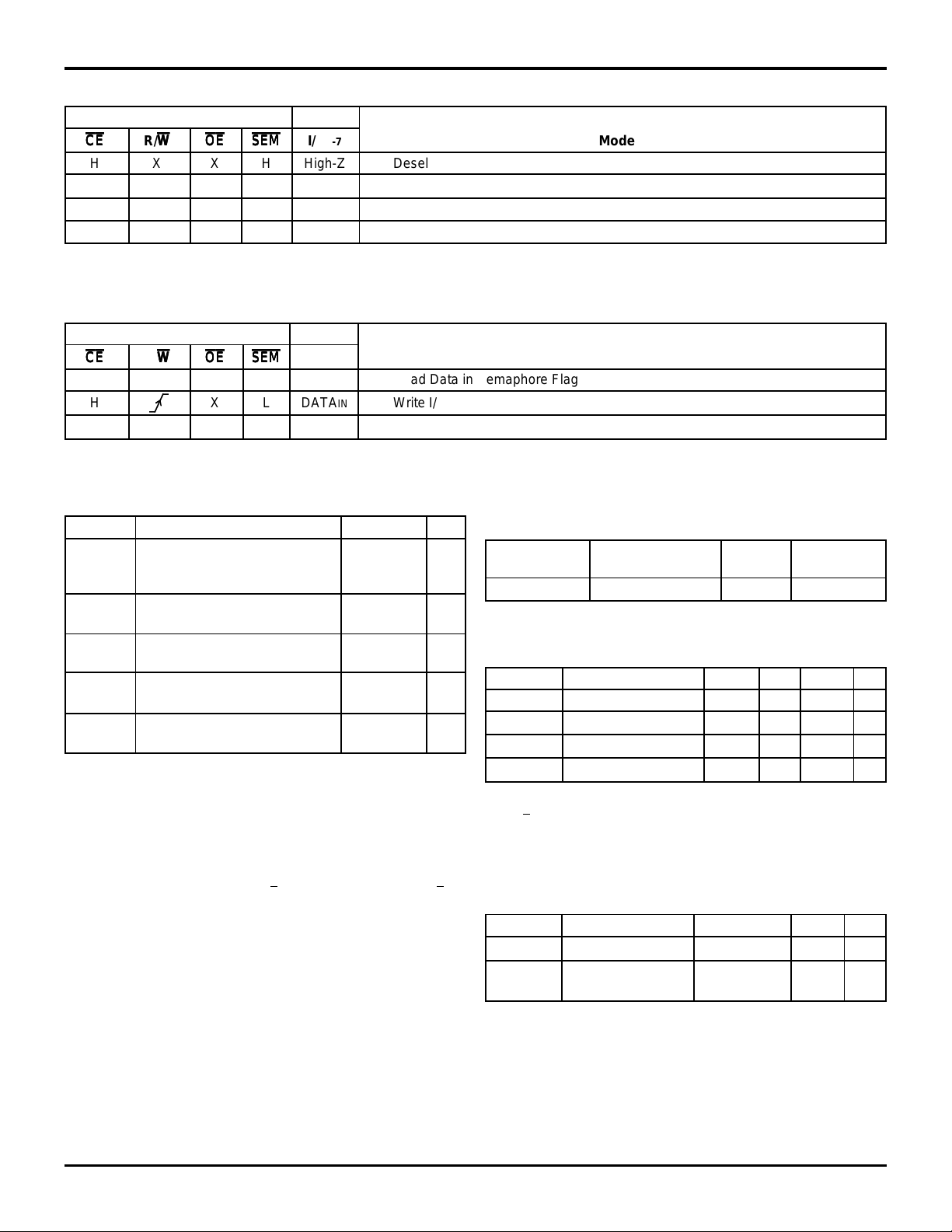
TRUTH TABLE I – NON-CONTENTION READ/WRITE CONTROL
Inputs
(1)
Outputs
CECE
CECE
CE
R/
WW
WW
W
OEOE
OEOE
OE
SEMSEM
SEMSEM
SEM
I/O
0-7 Mode
H X X H High-Z Deselected: Power-Down
L L X H DATA
IN Write to Memory
L H L H DATA
OUT Read Memory
X X H X High-Z Outputs Disabled
NOTE:
2943 tbl 02
1. A0L — A14L ≠ A0R — A14R.
TRUTH TABLE II – SEMAPHORE READ/WRITE CONTROL
(1)
Inputs Outputs
CECE
CECE
CE
R/
WW
WW
W
OEOE
OEOE
OE
SEMSEM
SEMSEM
SEM
I/O
0-7 Mode
H H L L DATA
OUT Read Data in Semaphore Flag
H X L DATA
IN Write I/O0 into Semaphore Flag
L X X L — Not Allowed
NOTE: 2943 tbl 03
1. There are eight semaphore flags written to via I/O0 and read from all I/O's (I/O0-I/O7). These eight semaphores are addressed by A0 - A2.
RECOMMENDED OPERATING
TEMPERATURE AND SUPPLY VOLTAGE
Ambient
Grade Temperature GND V
CC
Commercial 0°C to +70°C 0V 3.3V ± 0.3V
2943 tbl 05
ABSOLUTE MAXIMUM RATINGS
(1)
Symbol Rating Commercial Unit
V
TERM
(2)
Terminal Voltage –0.5 to +4.6 V
with Respect
to GND
T
A Operating 0 to +70 °C
Temperature
T
BIAS Temperature –55 to +125 °C
Under Bias
T
STG Storage –55 to +125 °C
Temperature
I
OUT DC Output 50 mA
Current
NOTES: 2943 tbl 04
1. Stresses greater than those listed under ABSOLUTE MAXIMUM
RATINGS may cause permanent damage to the device. This is a stress
rating only and functional operation of the device at these or any other
conditions above those indicated in the operational sections of this
specification is not implied. Exposure to absolute maximum rating
conditions for extended periods may affect reliability.
2. V
TERM must not exceed Vcc + 0.3V for more than 25% of the cycle time
or 10ns maximum, and is limited to
< 20mA for the period of VTERM > Vcc
+ 0.3V.
CAPACITANCE
(1)
(TA = +25°C, f = 1.0MHz)TQFP ONLY
Symbol Parameter Conditions
(2)
Max. Unit
C
IN Input Capacitance VIN = 3dV 9 pF
C
OUT Output VOUT = 3dV 10 pF
Capacitance
NOTES: 2943 tbl 07
1. This parameter is determined by device characterization but is not
production tested.
2. 3dV represents the interpolated capacitance when the input and output
signals switch from 0V to 3V or from 3V to 0V.
RECOMMENDED DC OPERATING
CONDITIONS
(2)
Symbol Parameter Min. Typ. Max. Unit
V
CC Supply Voltage 3.0 3.3 3.6 V
GND Supply Voltage 0 0 0 V
V
IH Input High Voltage 2.0 — VCC+0.3 V
V
IL Input Low Voltage –0.3
(1)
— 0.8 V
NOTES: 2943 tbl 06
1. VIL > -1.5V for pulse width less than 10ns.
2. V
TERM must not exceed Vcc + 0.3V.
IDT70V07S/L
HIGH-SPEED 3.3V 32K x 8 DUAL-PORT STATIC RAM COMMERCIAL TEMPERATURE RANGE
6.37 5
DC ELECTRICAL CHARACTERISTICS OVER THE
OPERATING TEMPERATURE AND SUPPLY VOLTAGE RANGE
(VCC = 3.3V ± 0.3V)
IDT70V07S IDT70V07L
Symbol Parameter Test Conditions Min. Max. Min. Max. Unit
|I
LI| Input Leakage Current
(1)
VCC = 3.6V, VIN = 0V to VCC —10—5µA
|I
LO| Output Leakage Current
CE
= VIH, VOUT = 0V to VCC —10—5µA
V
OL Output Low Voltage IOL = 4mA — 0.4 — 0.4 V
V
OH Output High Voltage IOH = -4mA 2.4 — 2.4 — V
2943 tbl 08
DC ELECTRICAL CHARACTERISTICS OVER THE
OPERATING TEMPERATURE AND SUPPLY VOLTAGE RANGE
(1)
(VCC = 3.3V ± 0.3V)
70V07X25 70V07X35 70V07X55
Test
Symbol Parameter Condition Version Typ.
(2)
Max. Typ.
(2)
Max. Typ.
(2)
Max. Unit
I
CC Dynamic Operating
CE
= VIL, Outputs Open COM’L. S 100 170 90 140 90 140 mA
Current
SEM
= V
IH L 100 140 90 120 90 120
(Both Ports Active) f = f
MAX
(3)
ISB1 Standby Current
CE
R =
CE
L = VIH COM’L. S 14 30 12 30 12 30 mA
(Both Ports — TTL
SEM
R =
SEM
L = VIH L12 24 10 24 10 24
Level Inputs) f = f
MAX
(3)
ISB2 Standby Current
CE
"A" = VIL and
CE
"B" = VIH
(5)
COM’L. S 50 95 45 87 45 87 mA
(One Port — TTL Active Port Outputs Open, L 50 85 45 75 45 75
Level Inputs) f = f
MAX
(3)
SEM
R =
SEM
L = VIH
ISB3 Full Standby Current Both Ports
CE
L and COM’L. S 1.0 6 1.0 6 1.0 6 mA
(Both Ports — All
CE
R > VCC - 0.2V L 0.2 3 0.2 3 0.2 3
CMOS Level Inputs) V
IN > VCC - 0.2V or
V
IN < 0.2V, f = 0
(4)
SEM
R =
SEM
L > VCC - 0.2V
I
SB4 Full Standby Current
CE
"A" < 0.2V and COM’L. S 60 90 55 85 55 85 mA
(One Port — All
CE
"B" > VCC - 0.2V
(5)
L60 80 55 74 55 74
CMOS Level Inputs)
SEM
R =
SEM
L > VCC - 0.2V
V
IN > VCC - 0.2V or VIN < 0.2V
Active Port Outputs Open
f = f
MAX
(3)
NOTES: 2943 tbl 09
1. "X" in part numbers indicates power rating (S or L).
2. V
CC = 3.3V, TA = +25°C, and are not production tested. ICCDC = 80mA (Typ.)
3. At f = f
MAX, address and control lines (except Output Enable) are cycling at the maximum frequency read cycle of 1 / tRC, and using “AC Test Conditions”
of input levels of GND to 3V.
4. f = 0 means no address or control lines change.
5. Port "A" may be either left or right port. Port "B" is the opposite from port "A".
NOTE:
1. At Vcc ≤ 2.0V input leakages are undefined.
6.37 6
IDT70V07S/L
HIGH-SPEED 3.3V 32K x 8 DUAL-PORT STATIC RAM COMMERCIAL TEMPERATURE RANGE
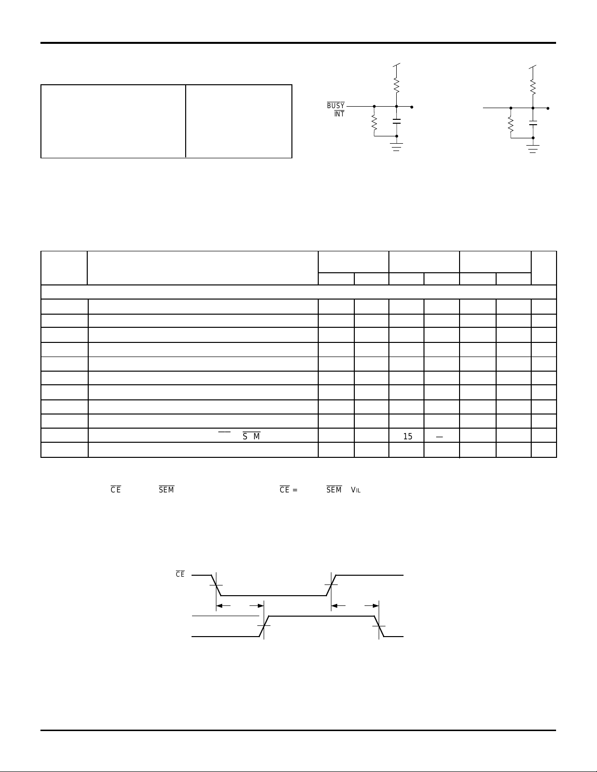
AC TEST CONDITIONS
Input Pulse Levels GND to 3.0V
Input Rise/Fall Times 5ns Max.
Input Timing Reference Levels 1.5V
Output Reference Levels 1.5V
Output Load Figures 1 and 2
2943 tbl 10
Figure 1. AC Output Test Load Figure 2. Output Test Load
(for t
LZ, tHZ, tWZ, tOW)
* Including scope and jig.
2943 drw 06
590Ω
30pF435Ω
3.3V
DATA
OUT
BUSY
INT
590Ω
5pF435Ω
3.3V
DATA
OUT
2943 drw 05
CE
2943 drw 07
t
PU
I
CC
I
SB
t
PD
50% 50%
TIMING OF POWER-UP POWER-DOWN
NOTES: 2943 tbl 11
1. Transition is measured ±200mV from Low or High-impedance voltage with Output Test Load (Figure 2).
2. This parameter is guaranteed by device characterization, but is not production tested.
3. To access RAM,
CE
= V
IL and
SEM
= VIH. To access semaphore,
CE
= VIH and
SEM
= VIL.
4. "X" in part numbers indicates power rating (S or L).
AC ELECTRICAL CHARACTERISTICS OVER THE
OPERATING TEMPERATURE AND SUPPLY VOLTAGE RANGE
(4)
IDT70V07X25 IDT70V07X35 IDT70V07X55
Symbol Parameter Min. Max. Min. Max. Min. Max. Unit
READ CYCLE
t
RC Read Cycle Time 25 — 35 — 55 — ns
t
AA Address Access Time — 25 — 35 — 55 ns
t
ACE Chip Enable Access Time
(3)
—25—35 —55ns
t
AOE Output Enable Access Time — 15 — 20 — 30 ns
t
OH Output Hold from Address Change 3 — 3 — 3 — ns
t
LZ Output Low-Z Time
(1, 2)
3—3— 3—ns
t
HZ Output High-Z Time
(1, 2)
—15—20 —25ns
t
PU Chip Enable to Power Up Time
(2)
0—0— 0—ns
t
PD Chip Disable to Power Down Time
(2)
—25—35 —50ns
t
SOP Semaphore Flag Update Pulse (
OE
or
SEM
)15—15—15—ns
t
SAA Semaphore Address Access Time — 35 — 45 — 65 ns
 Loading...