


Integrated Device Technology Inc. IDT54FCT240, IDT54FCT240A, IDT54FCT240C, IDT54FCT241, IDT54FCT241A User Manual
...
IDT54FCT2373AT
FAST CMOS OCTAL IDT54/74FCT373T/AT/CT/DT - 2373T/AT/CT |
||
TRANSPARENT |
IDT54/74FCT533T/AT/CT |
|
IDT54/74FCT573T/AT/CT/DT - 2573T/AT/CT |
||
LATCHES |
||
|
||
Integrated Device Technology, Inc.
FEATURES:
•Common features:
–Low input and output leakage ≤1μA (max.)
–CMOS power levels
–True TTL input and output compatibility
–VOH = 3.3V (typ.)
–VOL = 0.3V (typ.)
–Meets or exceeds JEDEC standard 18 specifications
–Product available in Radiation Tolerant and Radiation Enhanced versions
–Military product compliant to MIL-STD-883, Class B and DESC listed (dual marked)
–Available in DIP, SOIC, SSOP, QSOP, CERPACK and LCC packages
•Features for FCT373T/FCT533T/FCT573T:
–Std., A, C and D speed grades
–High drive outputs (-15mA IOH, 48mA IOL)
–Power off disable outputs permit “live insertion”
•Features for FCT2373T/FCT2573T:
–Std., A and C speed grades
– Resistor output (-15mA IOH, 12mA |
IOL Com.) |
(-12mA IOH, 12mA |
IOL Mil.) |
– Reduced system switching noise
DESCRIPTION:
The FCT373T/FCT2373T, FCT533T and FCT573T/ FCT2573T are octal transparent latches built using an advanced dual metal CMOS technology. These octal latches have 3-state outputs and are intended for bus oriented applications. The flip-flops appear transparent to the data when Latch Enable (LE) is HIGH. When LE is LOW, the data that meets the set-up time is latched. Data appears on the bus when the Output Enable (OE) is LOW. When OE is HIGH, the bus output is in the highimpedance state.
The FCT2373T and FCT2573T have balanced drive outputs with current limiting resistors. This offers low ground bounce, minimal undershoot and controlled output fall timesreducing the need for external series terminating resistors. The FCT2xxxT parts are plug-in replacements for FCTxxxT parts.
FUNCTIONAL BLOCK DIAGRAM IDT54/74FCT373T/2373T AND IDT54/74FCT573T/2573T
D0 |
|
D1 |
|
D2 |
|
D3 |
|
D4 |
|
D5 |
|
|
D6 |
|
D7 |
||||||||
|
|
|
|
|
|
|
|
|
|
|
|
|
|
|
|
|
|
|
|
|
|
|
|
|
D |
|
|
D |
|
|
D |
|
|
D |
|
|
D |
|
|
D |
|
|
|
D |
|
|
D |
|
|
O |
|
|
O |
|
|
O |
|
|
O |
|
|
O |
|
|
|
O |
|
|
O |
|
O |
|
|
G |
|
|
G |
|
|
G |
|
|
G |
|
|
G |
|
|
G |
|
|
G |
|
|
G |
LE
OE
O0 |
O1 |
O2 |
O3 |
O4 |
O5 |
O6 |
O7 |
2564 cnv* 01
FUNCTIONAL BLOCK DIAGRAM IDT54/74FCT533T
D0 |
D1 |
D2 |
|
D3 |
|
D4 |
|
D5 |
|
D6 |
D7 |
||||||||
|
|
|
|
|
|
|
|
|
|
|
|
|
|
|
|
|
|
|
|
|
D |
|
D |
|
D |
|
|
D |
|
|
D |
|
|
D |
|
|
D |
|
D |
|
O |
|
O |
|
|
O |
|
|
O |
|
|
O |
|
|
O |
|
O |
|
O |
|
G |
|
G |
|
G |
|
|
G |
|
|
G |
|
|
G |
|
|
G |
|
G |
LE
OE |
|
|
|
|
|
|
|
O0 |
O1 |
O2 |
O3 |
O4 |
O5 |
O6 |
O7 |
The IDT logo is a registered trademark of Integrated Device Technology, Inc. |
|
|
|
|
|
2564 cnv* 02 |
|
|
|
|
|
|
|
||
MILITARY AND COMMERCIAL TEMPERATURE RANGES |
|
|
|
|
AUGUST 1995 |
||
|
|
|
|
|
|
|
|
©1995 Integrated Device Technology, Inc. |
|
6.12 |
|
|
|
|
DSC-4216/6 |
1

IDT54/74FCT373T/AT/CT/DT - 2373T/AT/CT, IDT54/74FCT533T/AT/CT, IDT54/74FCT573T/AT/CT/DT - 2573T/AT/CT
FAST CMOS OCTAL TRANSPARENT LATCHES MILITARY AND COMMERCIAL TEMPERATURE RANGES
PIN CONFIGURATIONS
IDT54/74FCT373/2373T
OE |
|
1 |
|
20 |
|
VCC |
O0 |
|
2 |
|
19 |
|
O7 |
|
|
|
||||
D0 |
|
3 |
P20-1 |
18 |
|
D7 |
|
|
|||||
D1 |
|
4 |
17 |
|
D6 |
|
|
D20-1 |
|
||||
|
|
|
|
|
O6 |
|
O1 |
|
5 |
SO20-2 |
16 |
|
|
|
|
|||||
O2 |
|
6 |
SO20-7 |
15 |
|
O5 |
|
|
|||||
D2 |
|
7 |
SO20-8 |
14 |
|
D5 |
|
|
|||||
D3 |
|
8 |
& |
13 |
|
D4 |
|
|
|||||
|
E20-1 |
|
||||
O3 |
|
|
O4 |
|||
|
9 |
|
12 |
|
||
|
|
|
||||
GND |
|
10 |
|
11 |
|
LE |
|
|
|
2564 cnv* 03
DIP/SOIC/SSOP/QSOP/CERPACK
TOP VIEW
IDT54/74FCT573/2573T
OE |
1 |
|
20 |
VCC |
|
D0 |
2 |
|
19 |
O0 |
|
D1 |
3 |
P20-1 |
18 |
O1 |
|
D2 |
4 |
17 |
O2 |
||
D20-1 |
|||||
|
|
|
|
||
D3 |
5 |
SO20-2 |
16 |
O3 |
|
D4 |
6 |
SO20-7 |
15 |
O4 |
|
D5 |
7 |
SO20-8 |
14 |
O5 |
|
D6 |
8 |
& |
13 |
O6 |
|
E20-1 |
|||||
D7 |
9 |
|
12 |
O7 |
|
GND |
10 |
|
11 |
LE |
2564 cnv* 05
DIP/SOIC/SSOP/QSOP/CERPACK
TOP VIEW
IDT54/74FCT533
OE |
1 |
|
20 |
VCC |
|
O0 |
2 |
|
19 |
O7 |
|
D0 |
3 |
|
18 |
D7 |
|
D1 |
4 |
P20-1 |
17 |
D6 |
|
O1 |
|
|
|
||
5 |
D20-1 16 |
O6 |
|||
O2 |
6 |
SO20-2 15 |
O5 |
||
D2 |
7 |
& |
14 |
D5 |
|
E20-1 |
|||||
D3 |
8 |
13 |
D4 |
||
|
|||||
O3 |
9 |
|
12 |
O4 |
|
GND |
10 |
|
11 |
LE |
|
2564 cnv* 07
DIP/SOIC/CERPACK
TOP VIEW
INDEX |
D0 |
O0 |
OE VCC |
O7 |
|
|
|
||||
|
3 |
2 |
20 19 |
|
|
D1 |
4 |
|
1 |
18 |
D7 |
|
|
||||
O1 |
5 |
|
|
17 |
D6 |
O2 |
6 |
L20-2 |
16 |
O6 |
|
D2 |
7 |
|
|
15 |
O5 |
D3 |
8 |
|
|
14 |
D5 |
|
9 |
10 11 12 13 |
|
||
|
O3 |
GND |
LE O4 |
D4 |
|
|
|
|
LCC |
|
|
|
|
TOP VIEW |
|
|
|
INDEX |
D1 |
D0 |
OE VCC |
O0 |
|
|
|
||||
|
3 |
2 |
20 19 |
|
|
D2 |
4 |
|
1 |
18 |
O1 |
|
|
||||
D3 |
5 |
|
|
17 |
O2 |
D4 |
6 |
L20-2 |
16 |
O3 |
|
D5 |
7 |
|
|
15 |
O4 |
D6 |
8 |
|
|
14 |
O5 |
|
9 |
10 11 12 13 |
|
||
|
D7 |
GND |
LE O7 |
O6 |
|
|
|
|
LCC |
|
|
|
|
TOP VIEW |
|
|
|
INDEX |
D0 |
O0 |
OE |
VCC |
O7 |
|
|
|
|||||
|
3 |
2 |
20 19 |
|
||
D1 |
4 |
|
1 |
|
18 |
D7 |
|
|
|
||||
O1 |
5 |
|
|
|
17 |
D6 |
O2 |
6 |
L20-2 |
|
16 |
O6 |
|
D2 |
7 |
|
|
|
15 |
O5 |
D3 |
8 |
|
|
|
14 |
D5 |
|
9 |
10 11 12 13 |
|
|||
|
O3 |
GND |
LE |
O4 |
D4 |
|
|
|
|
LCC |
|
|
|
|
|
TOP VIEW |
|
|
||
2564 cnv* 04
2564 cnv* 06
2564 cnv* 08
6.12 |
2 |
IDT54/74FCT373T/AT/CT/DT - 2373T/AT/CT, IDT54/74FCT533T/AT/CT, IDT54/74FCT573T/AT/CT/DT - 2573T/AT/CT |
|
FAST CMOS OCTAL TRANSPARENT LATCHES |
MILITARY AND COMMERCIAL TEMPERATURE RANGES |
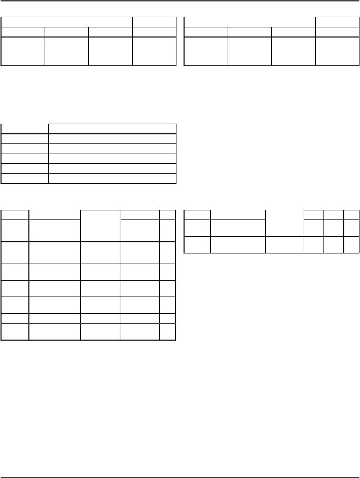
FUNCTION TABLE (533)(1) |
|
|
FUNCTION TABLE (373 and 573)(1) |
|
|||
|
Inputs |
|
Outputs |
|
Inputs |
|
Outputs |
DN |
LE |
OE |
ON |
DN |
LE |
OE |
ON |
H |
H |
L |
L |
H |
H |
L |
H |
L |
H |
L |
H |
L |
H |
L |
L |
X |
X |
H |
Z |
X |
X |
H |
Z |
NOTE: |
2564 tbl 01 NOTE: |
2564 tbl 02 |
1. H = HIGH Voltage Level |
1. H = HIGH Voltage Level |
|
L = LOW Voltage Level |
L = LOW Voltage Level |
|
X = Don’t Care |
X = Don’t Care |
|
Z = High Impedance |
Z = High Impedance |
|
DEFINITION OF FUNCTIONAL TERMS
Pin Names |
Description |
DN |
Data Inputs |
LE |
Latch Enable Input (Active HIGH) |
OE |
Output Enable Input (Active LOW) |
ON |
3-State Outputs |
ON |
Complementary 3-State Outputs |
|
2564 tbll 03 |
ABSOLUTE MAXIMUM RATINGS(1)
Symbol |
Rating |
Commercial |
Military |
Unit |
VTERM(2) |
Terminal Voltage |
–0.5 to +7.0 |
–0.5 to +7.0 |
V |
|
with Respect to |
|
|
|
|
GND |
|
|
|
VTERM(3) |
Terminal Voltage |
–0.5 to |
–0.5 to |
V |
|
with Respect to |
VCC +0.5 |
VCC +0.5 |
|
|
GND |
|
|
|
TA |
Operating |
0 to +70 |
–55 to +125 |
°C |
|
Temperature |
|
|
|
TBIAS |
Temperature |
–55 to +125 |
–65 to +135 |
°C |
|
Under Bias |
|
|
|
TSTG |
Storage |
–55 to +125 |
–65 to +150 |
°C |
|
Temperature |
|
|
|
PT |
Power Dissipation |
0.5 |
0.5 |
W |
IOUT |
DC Output |
–60 to +120 |
–60 to +120 |
mA |
|
Current |
|
|
|
NOTES: |
|
|
2564 lnk 04 |
|
1.Stresses greater than those listed under ABSOLUTE MAXIMUM RATINGS may cause permanent damage to the device. This is a stress rating only and functional operation of the device at these or any other conditions above those indicated in the operational sections of this specification is not implied. Exposure to absolute maximum rating conditions for extended periods may affect reliability. No terminal voltage may exceed VCC by +0.5V unless otherwise noted.
2.Input and VCC terminals only.
3.Outputs and I/O terminals only.
CAPACITANCE (TA = +25°C, f = 1.0MHz)
Symbol |
Parameter(1) |
Conditions |
Typ. |
Max. |
Unit |
CIN |
Input |
VIN = 0V |
6 |
10 |
pF |
|
Capacitance |
|
|
|
|
COUT |
Output |
VOUT = 0V |
8 |
12 |
pF |
|
Capacitance |
|
|
|
|
NOTE: |
|
|
|
2564 lnk 05 |
|
1. This parameter is measured at characterization but not tested.
6.12 |
3 |
 Loading...