


IDT IDT54FCT821AT, IDT54FCT821BT, IDT54FCT821CT, IDT54FCT823AT, IDT54FCT823BT User Manual
...IDT54/74FCT821AT/BIDT54FCT821ATD/CT, 823/825AT/BT/CT/DT |
|
|
||||||
|
|
|
|
|
|
|||
|
|
|
|
|
|
|
MILITARY AND COMMERCIAL TEMPERATURE RANGES |
|
HIGH-PERFORMANCE |
|
CMOS BUS INTERFACE REGISTERS |
||||||
|
|
|
|
|
|
HIGH-PERFORMANCE |
|
IDT54/74FCT821AT/BT/CT |
|
|
|
|
|
|
CMOS BUS |
|
IDT54/74FCT823AT/BT/CT/DT |
|
|
|
|
|
|
|
||
|
|
|
|
|
|
INTERFACE REGISTERS |
IDT54/74FCT825AT/BT/CT |
|
|
|
|
|
|
|
|
||
Integrated Device Technology, Inc.
FEATURES:
•Common features:
–Low input and output leakage ≤1μA (max.)
–CMOS power levels
–True TTL input and output compatibility
–VOH = 3.3V (typ.)
–VOL = 0.3V (typ.)
–Meets or exceeds JEDEC standard 18 specifications
–Product available in Radiation Tolerant and Radiation Enhanced versions
–Military product compliant to MIL-STD-883, Class B and DESC listed (dual marked)
–Available in DIP, SOIC, SSOP, QSOP, CERPACK and LCC packages
•Features for FCT821T/FCT823T/FCT825T:
–A, B, C and D speed grades
–High drive outputs (-15mA IOH, 48mA IOL)
–Power off disable outputs permit “live insertion”
DESCRIPTION:
The FCT82xT series is built using an advanced dual metal CMOS technology. The FCT82xT series bus interface registers are designed to eliminate the extra packages required to buffer existing registers and provide extra data width for wider address/data paths or buses carrying parity. The FCT821T are buffered, 10-bit wide versions of the popular FCT374T function. The FCT823T are 9-bit wide buffered registers with Clock Enable (EN) and Clear (CLR) – ideal for parity bus interfacing in high-performance microprogrammed systems. The FCT825T are 8-bit buffered registers with all the FCT823T controls plus multiple enables (OE1, OE2, OE3) to allow multiuser control of the interface, e.g., CS, DMA and RD/WR. They are ideal for use as an output port requiring high IOL/IOH.
The FCT82xT high-performance interface family can drive large capacitive loads, while providing low-capacitance bus loading at both inputs and outputs. All inputs have clamp diodes and all outputs are designed for low-capacitance bus loading in high-impedance state.
FUNCTIONAL BLOCK DIAGRAM
D0 |
DN |
EN
CLR |
|
|
|
D CL Q |
D CL Q |
|
CP Q |
CP Q |
CP |
|
|
OE |
|
|
|
Y0 |
YN |
|
|
2567 drw 01 |
The IDT logo is a registered trademark of Integrated Device Technology, Inc. |
|
|
MILITARY AND COMMERCIAL TEMPERATURE RANGES |
AUGUST 1995 |
|
©1995 Integrated Device Technology, Inc |
6.21 |
DSC-4202/5 |
|
6.21 |
1 |
1
IDT54/74FCT821AT/BT/CT, 823/825AT/BT/CT/DT HIGH-PERFORMANCE CMOS BUS INTERFACE REGISTERS
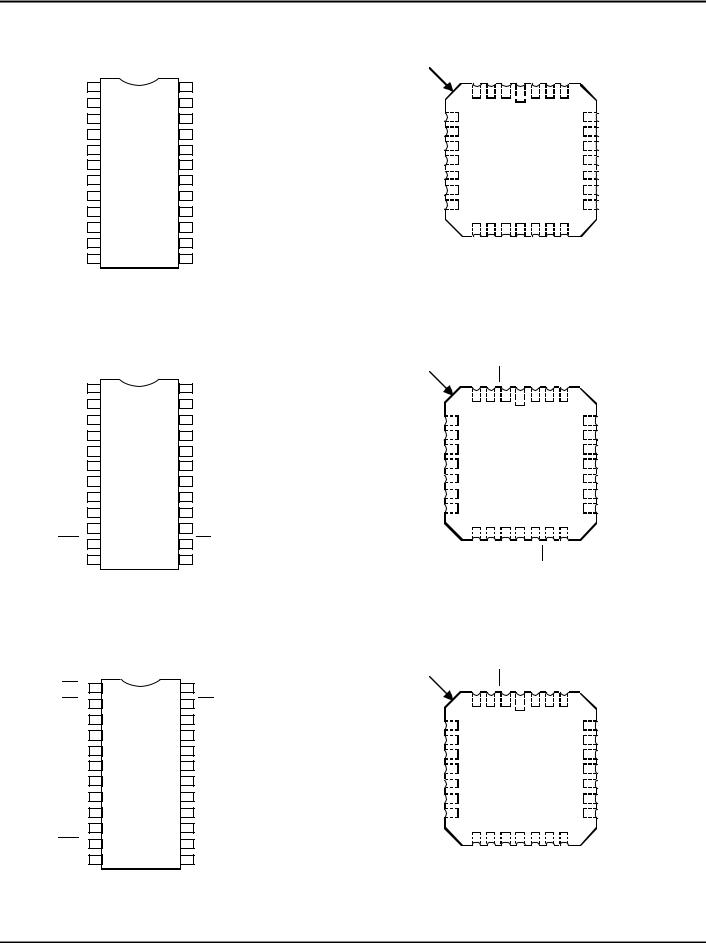
PIN CONFIGURATIONS
FCT821 10-BIT REGISTER
OE |
|
1 |
|
24 |
|
VCC |
D0 |
|
2 |
|
23 |
|
Y0 |
|
|
|
||||
D1 |
|
3 |
P24-1 |
22 |
|
Y1 |
|
|
|||||
D2 |
|
4 |
21 |
|
Y2 |
|
|
|
|||||
D3 |
|
5 |
D24-1 |
20 |
|
Y3 |
|
|
|||||
D4 |
|
6 |
SO24-2 19 |
|
Y4 |
|
|
|
|||||
|
|
|||||
D5 |
|
7 |
SO24-7 18 |
|
Y5 |
|
|
|
|||||
D6 |
|
8 |
SO24-8 17 |
|
Y6 |
|
|
|
|||||
|
|
|||||
D7 |
|
9 |
& |
16 |
|
Y7 |
|
|
|||||
|
E24-1 |
|
||||
D8 |
|
|
|
Y8 |
||
|
10 |
|
15 |
|
||
|
|
|
||||
D9 |
|
11 |
|
14 |
|
Y9 |
|
|
|
||||
GND |
|
12 |
|
13 |
|
CP |
|
|
|
||||
DIP/SOIC/SSOP/QSOP/CERPACK
TOP VIEW
FCT823 9-BIT REGISTER
OE |
|
1 |
|
24 |
|
VCC |
D0 |
|
2 |
|
23 |
|
Y0 |
|
|
|
||||
D1 |
|
3 |
P24-1 |
22 |
|
Y1 |
|
|
|||||
D2 |
|
4 |
21 |
|
Y2 |
|
|
|
|||||
D3 |
|
5 |
D24-1 |
20 |
|
Y3 |
|
|
|||||
|
|
|||||
D4 |
|
6 |
SO24-2 |
19 |
|
Y4 |
|
|
|||||
|
SO24-7 |
|
||||
|
|
18 |
|
|||
D5 |
|
7 |
SO24-8 |
|
Y5 |
|
|
|
|||||
D6 |
|
8 |
17 |
|
Y6 |
|
|
& |
|
||||
D7 |
|
9 |
16 |
|
Y7 |
|
|
E24-1 |
|
||||
D8 |
|
10 |
15 |
|
Y8 |
|
|
|
|
||||
|
|
|
||||
CLR |
|
11 |
|
14 |
|
EN |
|
|
|
||||
GND |
|
12 |
|
13 |
|
CP |
|
|
|
DIP/SOIC/SSOP/QSOP/CERPACK
TOP VIEW
FCT825 8-BIT REGISTER
OE1 |
|
1 |
|
24 |
|
VCC |
OE2 |
|
2 |
|
23 |
|
OE3 |
|
|
|
||||
D0 |
|
3 |
|
22 |
|
Y0 |
|
|
|
||||
D1 |
|
4 |
P24-1 |
21 |
|
Y1 |
|
|
|||||
D2 |
|
5 |
D24-1 |
20 |
|
Y2 |
|
|
|||||
D3 |
|
6 |
SO24-2 19 |
|
Y3 |
|
|
|
|||||
D4 |
|
7 |
SO24-8 18 |
|
Y4 |
|
|
|
|||||
D5 |
|
8 |
& |
17 |
|
Y5 |
|
|
|||||
D6 |
|
9 |
E24-1 |
16 |
|
Y6 |
|
|
|||||
|
|
|||||
D7 |
|
10 |
|
15 |
|
Y7 |
|
|
|
||||
CLR |
|
11 |
|
14 |
|
EN |
|
|
|
||||
GND |
|
12 |
|
13 |
|
CP |
|
|
|
||||
DIP/SOIC/QSOP/CERPACK
TOP VIEW
MILITARY AND COMMERCIAL TEMPERATURE RANGES
INDEX |
D1 |
D0 |
OE NC VCC Y0 Y1 |
|
||
|
|
|
|
|
|
|
D2 |
4 |
3 |
2 |
1 28 27 26 |
Y2 |
|
5 |
|
|
|
25 |
||
D3 |
6 |
|
|
|
24 |
Y3 |
D4 |
7 |
|
|
|
23 |
Y4 |
NC |
8 |
|
L28-1 |
22 |
NC |
|
D5 |
9 |
|
|
|
21 |
Y5 |
D6 |
10 |
|
|
|
20 |
Y6 |
D7 |
11 |
|
|
|
19 |
Y7 |
|
1213 14 15 16 17 18 |
|
||||
|
D8 |
D9 |
GND |
NC CP Y9 |
Y8 |
|
|
|
|
|
LCC |
|
|
|
|
TOP VIEW |
|
|
||
INDEX |
D1 D0 |
OE NC |
VCC Y0 Y1 |
|
|||
|
|
||||||
D2 |
4 |
3 |
2 |
1 |
28 27 26 |
Y2 |
|
5 |
|
|
|
|
25 |
||
D3 |
6 |
|
|
|
|
24 |
Y3 |
D4 |
7 |
|
|
|
|
23 |
Y4 |
NC |
8 |
|
L28-1 |
22 |
NC |
||
D5 |
9 |
|
|
|
|
21 |
Y5 |
D6 |
10 |
|
|
|
|
20 |
Y6 |
D7 |
11 |
|
|
|
|
19 |
Y7 |
|
1213 14 15 16 17 18 |
|
|||||
|
D8 |
CLR |
GND |
NC |
CP EN |
Y8 |
|
|
|
|
|
LCC |
|
|
|
|
|
TOP VIEW |
|
|
|||
INDEX |
D0 |
OE2 |
OE1 |
NC |
VCC OE3 |
Y0 |
|
|
|
|
|
|
|
|
|
D1 |
4 |
3 |
2 |
1 |
28 27 26 |
Y1 |
|
5 |
|
|
|
|
25 |
||
D2 |
6 |
|
|
|
|
24 |
Y2 |
D3 |
7 |
|
|
|
|
23 |
Y3 |
NC |
8 |
|
L28-1 |
22 |
NC |
||
D4 |
9 |
|
|
|
|
21 |
Y4 |
D5 |
10 |
|
|
|
|
20 |
Y5 |
D6 |
11 |
|
|
|
|
19 |
Y6 |
|
1213 14 15 16 17 18 |
|
|||||
|
D7 |
CLR |
GND |
NC |
CP EN Y7 |
|
|
|
|
|
|
LCC |
|
|
|
|
|
TOP VIEW |
|
|
|||
2567 drw 02
2567 drw 03
2567 drw 04
6.21 |
2 |

IDT54/74FCT821AT/BT/CT, 823/825AT/BT/CT/DT |
|
HIGH-PERFORMANCE CMOS BUS INTERFACE REGISTERS |
MILITARY AND COMMERCIAL TEMPERATURE RANGES |
PIN DESCRIPTION
Names |
I/O |
Description |
DI |
I |
The D flip-flop data inputs. |
CLR |
I |
When the clear input is LOW and OE is |
|
|
LOW, the QI outputs are LOW. When |
|
|
the clear input is HIGH, data can be |
|
|
entered into the register. |
CP |
I |
Clock Pulse for the Register; enters |
|
|
data into the register on the LOW-to- |
|
|
HIGH transition. |
YI |
O |
The register 3-state outputs. |
EN |
I |
Clock Enable. When the clock enable is |
|
|
LOW, data on the D I input is transferred |
|
|
to the QI output on the LOW-to-HIGH |
|
|
clock transition. When the clock enable |
|
|
is HIGH, the QI outputs do not change |
|
|
state, regardless of the data or clock |
|
|
input transitions. |
OE |
I |
Output Control. When the OE input is |
|
|
HIGH, the Y I outputs are in the high- |
|
|
impedance state. When the OE input is |
|
|
LOW, the TRUE register data is present |
|
|
at the YI outputs. |
|
|
2567 tbl 01 |
FUNCTION TABLE(1)
|
|
Inputs |
|
|
Internal/ |
|
|
|
|
|
|
Outputs |
|
||
|
|
|
|
|
|
||
OE |
CLR |
EN |
DI |
CP |
QI |
YI |
Function |
H |
H |
L |
L |
− |
L |
Z |
High Z |
H |
H |
L |
H |
− |
H |
Z |
|
H |
L |
X |
X |
X |
L |
Z |
Clear |
L |
L |
X |
X |
X |
L |
L |
|
H |
H |
H |
X |
X |
NC |
Z |
Hold |
L |
H |
H |
X |
X |
NC |
NC |
|
H |
H |
L |
L |
− |
L |
Z |
Load |
H |
H |
L |
H |
− |
H |
Z |
|
L |
H |
L |
L |
− |
L |
L |
|
L |
H |
L |
H |
− |
H |
H |
|
NOTE: |
|
|
|
|
|
|
2567 tbl 02 |
1.H = HIGH L = LOW
X = Don’t Care
NC = No Change
− = LOW-to-HIGH Transition Z = High Impedance
ABSOLUTE MAXIMUM RATINGS(1)
Symbol |
Rating |
Commercial |
Military |
Unit |
VTERM(2) |
Terminal Voltage |
–0.5 to +7.0 |
–0.5 to +7.0 |
V |
|
with Respect to |
|
|
|
|
GND |
|
|
|
VTERM(3) |
Terminal Voltage |
–0.5 to |
–0.5 to |
V |
|
with Respect to |
VCC +0.5 |
VCC +0.5 |
|
|
GND |
|
|
|
TA |
Operating |
0 to +70 |
–55 to +125 |
°C |
|
Temperature |
|
|
|
TBIAS |
Temperature |
–55 to +125 |
–65 to +135 |
°C |
|
Under Bias |
|
|
|
TSTG |
Storage |
–55 to +125 |
–65 to +150 |
°C |
|
Temperature |
|
|
|
PT |
Power Dissipation |
0.5 |
0.5 |
W |
IOUT |
DC Output |
–60 to +120 |
–60 to +120 |
mA |
|
Current |
|
|
|
NOTES: |
2567 lnk 03 |
|
1.Stresses greater than those listed under ABSOLUTE MAXIMUM RATINGS may cause permanent damage to the device. This is a stress rating only and functional operation of the device at these or any other conditions above those indicated in the operational sections of this specification is not implied. Exposure to absolute maximum rating conditions for extended periods may affect reliability. No terminal voltage may exceed VCC by +0.5V unless otherwise noted.
2.Input and VCC terminals only.
3.Outputs and I/O terminals only.
CAPACITANCE (TA = +25°C, f = 1.0MHz)
Symbol |
Parameter(1) |
Conditions |
Typ. |
Max. |
Unit |
CIN |
Input |
VIN = 0V |
6 |
10 |
pF |
|
Capacitance |
|
|
|
|
COUT |
Output |
VOUT = 0V |
8 |
12 |
pF |
|
Capacitance |
|
|
|
|
NOTE: |
|
|
|
2567 lnk 04 |
|
1. This parameter is measured at characterization but not tested.
6.21 |
3 |
 Loading...