


Integrated Device Technology Inc IDT7133SA20F, IDT7133SA20G, IDT7133SA20J, IDT7133SA20PF, IDT7133SA25F Datasheet
...
HIGH-SPEED
2K x 16 CMOS DUAL-PORT STATIC RAMS
Integrated Device Technology, Inc.
IDT7133SA/LA
IDT7143SA/LA
FEATURES:
•High-speed access
—Military: 25/35/45/55/70/90ns (max.)
—Commercial: 20/25/35/45/55/70/90ns (max.)
•Low-power operation
—IDT7133/43SA Active: 500 mW (typ.) Standby: 5mW (typ.)
—IDT7133/43LA Active: 500mW (typ.) Standby: 1mW (typ.)
•Versatile control for write: separate write control for lower and upper byte of each port
•MASTER IDT7133 easily expands data bus width to 32 bits or more using SLAVE IDT7143
•On-chip port arbitration logic (IDT7133 only)
•BUSY output flag on IDT7133; BUSY input on IDT7143
•Fully asynchronous operation from either port
•Battery backup operation–2V data retention
•TTL-compatible; single 5V (±10%) power supply
•Available in 68-pin ceramic PGA, 68-pin Flatpack, 68-pin PLCC, and 100-pin TQFP
•Military product compliant to MIL-STD-883, Class B
•Industrial temperature range (–40°C to +85°C) is available, tested to military electrical specifications
DESCRIPTION:
The IDT7133/7143 are high-speed 2K x 16 Dual-Port Static RAMs. The IDT7133 is designed to be used as a stand-alone 16-bit Dual-Port RAM or as a “MASTER” Dual-Port RAM together with the IDT7143 “SLAVE” Dual-Port in 32-bit-or- more word width systems. Using the IDT MASTER/SLAVE Dual-Port RAM approach in 32-bit-or-wider memory system applications results in full-speed, error-free operation without the need for additional discrete logic.
Both devices provide two independent ports with separate control, address, and I/O pins that permit independent, asynchronous access for reads or writes to any location in memory. An automatic power down feature, controlled by CE, permits the on-chip circuitry of each port to enter a very low standby power mode.
Fabricated using IDT’s CMOS high-performance technology, these devices typically operate on only 500mW of power. Low-power (LA) versions offer battery backup data retention capability, with each port typically consuming 200μW for a 2V battery.
The IDT7133/7143 devices have identical pinouts. Each is packaged in a 68-pin ceramic PGA, a 68-pin flatpack, a 68-pin PLCC, and a 100-pin TQFP. Military grade product is manufactured in compliance with the latest revision of MIL-STD- 883, Class B, making it ideally suited to military temperature applications demanding the highest level of performance and reliability.
FUNCTIONAL BLOCK DIAGRAM |
|
|
|
|
(2) |
|
|
|
(2) |
R/WLUB |
|
|
|
R/WRUB |
CEL |
|
|
|
CER |
(2) |
|
|
|
R/WRLB(2) |
R/WLLB |
|
|
|
|
OEL |
|
|
|
OER |
I/O8L - I/O15L |
|
I/O |
I/O |
I/O8R - I/O15R |
|
|
|
||
I/O0L - I/O7L |
|
CONTROL |
CONTROL |
I/O0R - I/O7R |
(1) |
|
|
|
(1) |
|
|
|
BUSYR |
|
BUSYL |
|
|
|
|
A10L |
ADDRESS |
MEMORY |
|
A10R |
|
|
ADDRESS |
||
A0L |
DECODER |
ARRAY |
|
DECODER |
|
|
|
A0R |
|
NOTES: |
|
|
|
|
1. IDT7133 (MASTER): BUSY is |
|
11 |
|
11 |
open drain output and requires |
|
|
|
|
pull-up resistor of 270Ω. |
CEL |
ARBITRATION |
CER |
|
IDT7143 (SLAVE): BUSY is |
LOGIC |
|
||
|
(IDT7133 ONLY) |
|
||
input. |
|
|
||
2. "LB" designates "Lower Byte" |
|
|
|
|
and "UB" designates "Upper |
|
|
|
|
Byte" for the R/W signals. |
|
|
|
2746 drw 01 |
|
|
|
|
|
The IDT logo is a registered trademark of Integrated Device Technology, Inc.
MILITARY AND COMMERCIAL TEMPERATURE RANGES |
OCTOBER 1996 |
|
©1996 Integrated Device Technology, Inc. |
For latest information contact IDT’s web site at www.idt.com or fax-on-demand at 408-492-8391. |
DSC-2746/6 |
6.14 |
1 |
IDT7133SA/LA, IDT7143SA/LA |
|
HIGH-SPEED 2K x 16 DUAL-PORT RAMS |
MILITARY AND COMMERCIAL TEMPERATURE RANGES |
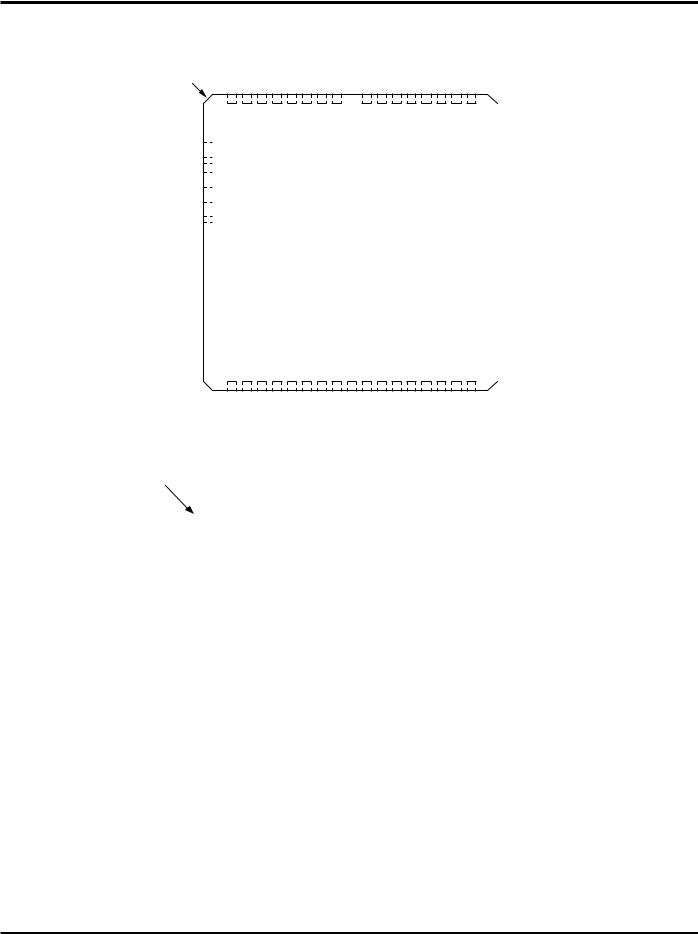
PIN CONFIGURATIONS(1,2)
INDEX |
I/O8L |
|
|
|
9 |
I/O9L  10
10
I/O10L  11
11
I/O11L  12
12
I/O12L 
 13
13
I/O13L  14
14
I/O14L  15
15
I/O15L  16
16
VCC  17
17
GND  18
18
I/O0R  19
19
I/O1R  20
20
I/O2R  21
21
I/O3R  22
22
I/O4R  23
23
I/O5R  24
24
I/O6R  25
25
I/O7R  26
26
27
I/O8R
INDEX 9L 8L 7L I/O I/O I/O
|
I/O7L |
|
I/O6L |
I/O5L |
I/O4L |
I/O3L |
I/O2L |
|
I/O1L |
|
|
I/O0L |
VCC R/WLUB |
R/WLLB |
OEL |
A10L |
|
A9L A8L |
A7L |
|
|
||||||||||||||||||||||||||||||||||||
8 |
7 |
|
6 |
5 |
4 |
|
3 |
2 |
|
|
|
|
|
68 67 66 65 |
|
64 63 62 61 |
|
|
|
A6L |
|||||||||||||||||||||||||||||||||||||
|
|
|
|
|
|
|
|
|
|
|
|||||||||||||||||||||||||||||||||||||||||||||||
|
|
|
|
|
|
|
|
|
|
|
|||||||||||||||||||||||||||||||||||||||||||||||
|
|
|
|
|
|
|
|
|
|
|
|
|
|
|
|
|
|
|
|
|
|
|
1 |
|
|
|
|
|
|
|
|
|
|
|
|
|
|
|
|
|
|
|
|
|
|
|
|
|
60 |
|
|||||||
|
|
|
|
|
|
|
|
|
|
|
|
|
|
|
|
|
|
|
|
|
|
|
|
|
|
|
|
|
|
|
|
|
|
|
|
|
|
|
|
|
|
|
|
|
|
|
|
|
|||||||||
|
|
|
|
|
|
|
|
|
|
|
|
|
|
|
|
|
|
|
|
|
|
|
|
|
|
|
|
|
|
|
|
|
|
|
|
|
|
|
|
|
|
|
|
|
|
|
|
59 |
|
A5L |
|||||||
|
|
|
|
|
|
|
|
|
|
|
|
|
|
|
|
|
|
|
|
|
|
|
|
|
|
|
|
|
|
|
|
|
|
|
|
|
|
|
|
|
|
|
|
|
|
|
|
|
|
|
|
||||||
|
|
|
|
|
|
|
|
|
|
|
|
|
|
|
|
|
|
|
|
|
|
|
|
|
|
|
|
|
|
|
|
|
|
|
|
|
|
|
|
|
|
|
|
|
|
|
|
|
|
|
|
||||||
|
|
|
|
|
|
|
|
|
|
|
|
|
|
|
|
|
|
|
|
|
|
|
|
|
|
|
|
|
|
|
|
|
|
|
|
|
|
|
|
|
|
|
|
|
|
|
|
|
|
|
58 |
|
A4L |
||||
|
|
|
|
|
|
|
|
|
|
|
|
|
|
|
|
|
|
|
|
|
|
|
|
|
|
|
|
|
|
|
|
|
|
|
|
|
|
|
|
|
|
|
|
|
|
|
|
|
|
|
|
||||||
|
|
|
|
|
|
|
|
|
|
|
|
|
|
|
|
|
|
|
|
|
|
|
|
|
|
|
|
|
|
|
|
|
|
|
|
|
|
|
|
|
|
|
|
|
|
|
|
|
|
|
|
||||||
|
|
|
|
|
|
|
|
|
|
|
|
|
|
|
|
|
|
|
|
|
|
|
|
|
|
|
|
|
|
|
|
|
|
|
|
|
|
|
|
|
|
|
|
|
|
|
|
|
|
|
57 |
|
A3L |
||||
|
|
|
|
|
|
|
|
|
|
|
|
|
|
|
|
|
|
|
|
|
|
|
|
|
|
|
|
|
|
|
|
|
|
|
|
|
|
|
|
|
|
|
|
|
|
|
|
|
|
|
|
||||||
|
|
|
|
|
|
|
|
|
|
|
|
|
|
|
|
|
|
|
|
|
|
|
|
|
|
|
|
|
|
|
|
|
|
|
|
|
|
|
|
|
|
|
|
|
|
|
|
|
|
|
|
||||||
|
|
|
|
|
|
|
|
|
|
|
|
|
|
|
|
|
|
|
|
|
|
|
|
|
|
|
|
|
|
|
|
|
|
|
|
|
|
|
|
|
|
|
|
|
|
|
|
|
|
|
56 |
|
A2L |
||||
|
|
|
|
|
|
|
|
|
|
|
|
|
|
|
|
|
|
|
|
|
|
|
|
|
|
|
|
|
|
|
|
|
|
|
|
|
|
|
|
|
|
|
|
|
|
|
|
|
|
|
|
||||||
|
|
|
|
|
|
|
|
|
|
|
|
|
|
|
|
|
|
|
|
|
|
|
|
|
|
|
|
|
|
|
|
|
|
|
|
|
|
|
|
|
|
|
|
|
|
|
|
|
|
|
|
||||||
|
|
|
|
|
|
|
|
|
|
|
|
|
|
|
|
|
|
|
|
|
|
|
|
|
|
|
|
|
|
|
|
|
|
|
|
|
|
|
|
|
|
|
|
|
|
|
|
|
|
|
55 |
|
A1L |
||||
|
|
|
|
|
|
|
|
|
|
|
|
|
|
|
|
|
|
|
|
|
|
|
|
|
|
|
|
|
|
|
|
|
|
|
|
|
|
|
|
|
|
|
|
|
|
|
|
|
|
|
|
||||||
|
|
|
|
|
|
|
|
|
|
|
|
|
|
|
|
|
|
|
|
|
|
|
|
|
|
|
|
|
|
|
|
|
|
|
|
|
|
|
|
|
|
|
|
|
|
|
|
|
|
|
|
||||||
|
|
|
|
|
|
|
|
|
|
|
|
|
|
|
|
|
|
|
|
IDT7133/43 |
|
|
|
|
|
|
|
|
|
|
|
|
|
|
|
|
|
|
54 |
|
A0L |
||||||||||||||||
|
|
|
|
|
|
|
|
|
|
|
|
|
|
|
|
|
|
|
|
|
|
|
|
|
|
|
|
|
|
|
|
|
|
|
|
|
|
|
|||||||||||||||||||
|
|
|
|
|
|
|
|
|
|
|
|
|
|
|
|
|
|
|
|
|
|
J68-1 |
|
|
|
|
|
|
|
|
|
|
|
|
|
|
|
|
|
|
53 |
|
BUSYL |
||||||||||||||
|
|
|
|
|
|
|
|
|
|
|
|
|
|
|
|
|
|
|
|
|
|
|
& |
|
|
|
|
|
|
|
|
|
|
|
|
|
|
|
|
|
|
|
|
|
|
|
|
|
|
||||||||
|
|
|
|
|
|
|
|
|
|
|
|
|
|
|
|
|
|
|
|
|
|
|
|
|
|
|
|
|
|
|
|
|
|
|
|
|
|
|
|
|
|
|
|
|
|
|
|
|
|||||||||
|
|
|
|
|
|
|
|
|
|
|
|
|
|
|
|
|
|
|
|
|
|
F68-1 |
|
|
|
|
|
|
|
|
|
|
|
|
|
|
|
|
|
|
52 |
|
CEL |
||||||||||||||
|
|
|
|
|
|
|
|
|
|
|
|
|
|
|
|
|
|
|
|
|
|
|
|
|
|
|
|
|
|
|
|
|
|
|
|
|
|
|
|
|
|
|
|
|
|
|
|
|
|
|
|
||||||
|
|
|
|
|
|
|
|
|
|
|
|
|
|
|
|
PLCC/FLATPACK |
|
|
|
|
|
|
|
|
|
|
|
|
|
|
|
|
|
|
51 |
|
CER |
||||||||||||||||||||
|
|
|
|
|
|
|
|
|
|
|
|
|
|
|
|
|
|
|
|
|
|
|
|
|
|
|
|
|
|
|
|
|
|
|
|||||||||||||||||||||||
|
|
|
|
|
|
|
|
|
|
|
|
|
|
|
|
|
|
|
TOP VIEW(3) |
|
|
|
|
|
|
|
|
|
|
|
|
|
|
|
|
|
|
50 |
|
BUSYR |
|||||||||||||||||
|
|
|
|
|
|
|
|
|
|
|
|
|
|
|
|
|
|
|
|
|
|
|
|
|
|
|
|
|
|
|
|
|
|
|
|
|
|
||||||||||||||||||||
|
|
|
|
|
|
|
|
|
|
|
|
|
|
|
|
|
|
|
|
|
|
|
|
|
|
|
|
|
|
|
|
|
|
|
|
|
|
||||||||||||||||||||
|
|
|
|
|
|
|
|
|
|
|
|
|
|
|
|
|
|
|
|
|
|
|
|
|
|
|
|
|
|
|
|
|
|
|
|
|
|
|
|
|
|
|
|
|
|
|
|
|
|
|
49 |
|
A0R |
||||
|
|
|
|
|
|
|
|
|
|
|
|
|
|
|
|
|
|
|
|
|
|
|
|
|
|
|
|
|
|
|
|
|
|
|
|
|
|
|
|
|
|
|
|
|
|
|
|
|
|
|
|
||||||
|
|
|
|
|
|
|
|
|
|
|
|
|
|
|
|
|
|
|
|
|
|
|
|
|
|
|
|
|
|
|
|
|
|
|
|
|
|
|
|
|
|
|
|
|
|
|
|
|
|
|
48 |
|
A1R |
||||
|
|
|
|
|
|
|
|
|
|
|
|
|
|
|
|
|
|
|
|
|
|
|
|
|
|
|
|
|
|
|
|
|
|
|
|
|
|
|
|
|
|
|
|
|
|
|
|
|
|
|
|
||||||
|
|
|
|
|
|
|
|
|
|
|
|
|
|
|
|
|
|
|
|
|
|
|
|
|
|
|
|
|
|
|
|
|
|
|
|
|
|
|
|
|
|
|
|
|
|
|
|
|
|
|
47 |
|
A2R |
||||
|
|
|
|
|
|
|
|
|
|
|
|
|
|
|
|
|
|
|
|
|
|
|
|
|
|
|
|
|
|
|
|
|
|
|
|
|
|
|
|
|
|
|
|
|
|
|
|
|
|
|
|
||||||
|
|
|
|
|
|
|
|
|
|
|
|
|
|
|
|
|
|
|
|
|
|
|
|
|
|
|
|
|
|
|
|
|
|
|
|
|
|
|
|
|
|
|
|
|
|
|
|
|
|
|
|
||||||
|
|
|
|
|
|
|
|
|
|
|
|
|
|
|
|
|
|
|
|
|
|
|
|
|
|
|
|
|
|
|
|
|
|
|
|
|
|
|
|
|
|
|
|
|
|
|
|
|
|
|
46 |
|
A3R |
||||
|
|
|
|
|
|
|
|
|
|
|
|
|
|
|
|
|
|
|
|
|
|
|
|
|
|
|
|
|
|
|
|
|
|
|
|
|
|
|
|
|
|
|
|
|
|
|
|
|
|
|
|
||||||
|
|
|
|
|
|
|
|
|
|
|
|
|
|
|
|
|
|
|
|
|
|
|
|
|
|
|
|
|
|
|
|
|
|
|
|
|
|
|
|
|
|
|
|
|
|
|
|
|
|
|
|
||||||
|
|
|
|
|
|
|
|
|
|
|
|
|
|
|
|
|
|
|
|
|
|
|
|
|
|
|
|
|
|
|
|
|
|
|
|
|
|
|
|
|
|
|
|
|
|
|
|
|
|
|
45 |
|
A4R |
||||
|
|
|
|
|
|
|
|
|
|
|
|
|
|
|
|
|
|
|
|
|
|
|
|
|
|
|
|
|
|
|
|
|
|
|
|
|
|
|
|
|
|
|
|
|
|
|
|
|
|
|
|
||||||
|
|
|
|
|
|
|
|
|
|
|
|
|
|
|
|
|
|
|
|
|
|
|
|
|
|
|
|
|
|
|
|
|
|
|
|
|
|
|
|
|
|
|
|
|
|
|
|
|
|
|
|
||||||
|
|
|
|
|
|
|
|
|
|
|
|
|
|
|
|
|
|
|
|
|
|
|
|
|
|
|
|
|
|
|
|
|
|
|
|
|
|
|
|
|
|
|
|
|
|
|
|
|
|
|
44 |
|
A5R |
||||
|
|
|
|
|
|
|
|
|
|
|
|
|
|
|
|
|
|
|
|
|
|
|
|
|
|
|
|
|
|
|
|
|
|
|
|
|
|
|
|
|
|
|
|
|
|
|
|
|
|
|
|
||||||
28 29 30 31 |
32 33 34 35 |
|
36 37 38 39 |
|
40 41 42 43 |
|
|
|
|
||||||||||||||||||||||||||||||||||||||||||||||||
|
I/O9R |
|
I/O10R |
I/O11R |
|
I/O12R |
|
I/O13R |
I/O14R |
|
I/O15R |
|
GND R/WRUB R/WRLB |
ROE |
|
A10R |
A9R |
|
A8R |
A7R |
A6R |
|
2746 drw 02 |
||||||||||||||||||||||||||||||||||
I/O6L |
I/O5L I/O4L |
I/O3L |
I/O2L GND I/O1L |
I/O0L |
OEL |
VCC R/WLLB |
N/C CEL R/WLUB N/C N/C |
N/C |
A10L A9L |
A8L |
A7L A6L |
|
|
||||||||||||||||||||||||||||||||||||||||||||
|
|
|
|
|
|
|
|
|
|
|
|
|
|
|
|
|
|
|
|
|
|
|
|
|
|
|
|
|
|
|
|
|
|
|
|
|
|
|
|
|
|
|
|
|
|
|
|
|
|
|
|
|
|
|
|
|
|
|
|
|
|
|
|
|
|
|
|
|
|
|
|
|
|
|
|
|
|
|
|
|
|
|
|
|
|
|
|
|
|
|
|
|
|
|
|
|
|
|
|
|
|
|
|
|
|
|
|
|
|
|
|
|
|
|
|
|
|
|
|
|
|
|
|
|
|
|
|
|
|
|
|
|
|
|
|
|
|
|
|
|
|
|
|
|
|
|
|
|
|
|
|
|
|
|
|
|
|
|
|
|
|
|
|
|
|
|
|
|
|
|
N/C |
|
100 99 98 97 96 95 94 93 92 91 90 89 88 87 86 85 84 83 82 81 80 79 78 77 76 |
|
|
N/C |
|||||||||||||||||||||||||||||||||||||||||||||||||
|
1 |
|
|
|
|
|
|
|
|
|
|
|
|
|
|
|
|
|
|
|
|
|
|
|
|
|
|
|
|
|
|
75 |
|
|||||||||||||||||||||
|
|
|
|
|
|
|
|
|
|
|
|
|
|
|
|
|
|
|
|
|
|
|
|
|
|
|
|
|
|
|
|
|||||||||||||||||||||||
N/C |
|
2 |
|
|
|
|
|
|
|
|
|
|
|
|
|
|
|
|
|
|
|
|
|
|
|
|
|
|
|
|
|
|
74 |
|
N/C |
|||||||||||||||||||
|
|
|
|
|
|
|
|
|
|
|
|
|
|
|
|
|
|
|
|
|
|
|
|
|
|
|
|
|
|
|
||||||||||||||||||||||||
|
|
|
|
|
|
|
|
|
|
|
|
|
|
|
|
|
|
|
|
|
|
|
|
|
|
|
|
|
|
|
|
|||||||||||||||||||||||
|
|
|
|
|
|
|
|
|
|
|
|
|
|
|
|
|
|
|
|
|
|
|
|
|
|
|
|
|
|
|
|
|||||||||||||||||||||||
N/C |
|
3 |
|
|
|
|
|
|
|
|
|
|
|
|
|
|
|
|
|
|
|
|
|
|
|
|
|
|
|
|
|
|
73 |
|
N/C |
|||||||||||||||||||
|
|
|
|
|
|
|
|
|
|
|
|
|
|
|
|
|
|
|
|
|
|
|
|
|
|
|
|
|
|
|
||||||||||||||||||||||||
|
|
|
|
|
|
|
|
|
|
|
|
|
|
|
|
|
|
|
|
|
|
|
|
|
|
|
|
|
|
|
|
|||||||||||||||||||||||
|
|
|
|
|
|
|
|
|
|
|
|
|
|
|
|
|
|
|
|
|
|
|
|
|
|
|
|
|
|
|
|
|||||||||||||||||||||||
N/C |
|
4 |
|
|
|
|
|
|
|
|
|
|
|
|
|
|
|
|
|
|
|
|
|
|
|
|
|
|
|
|
|
|
72 |
|
N/C |
|||||||||||||||||||
|
|
|
|
|
|
|
|
|
|
|
|
|
|
|
|
|
|
|
|
|
|
|
|
|
|
|
|
|
|
|
||||||||||||||||||||||||
|
|
|
|
|
|
|
|
|
|
|
|
|
|
|
|
|
|
|
|
|
|
|
|
|
|
|
|
|
|
|
|
|||||||||||||||||||||||
|
|
|
|
|
|
|
|
|
|
|
|
|
|
|
|
|
|
|
|
|
|
|
|
|
|
|
|
|
|
|
|
|||||||||||||||||||||||
I/O10L |
|
5 |
|
|
|
|
|
|
|
|
|
|
|
|
|
|
|
|
|
|
|
|
|
|
|
|
|
|
|
|
|
|
71 |
|
A5L |
|||||||||||||||||||
|
|
|
|
|
|
|
|
|
|
|
|
|
|
|
|
|
|
|
|
|
|
|
|
|
|
|
|
|
|
|
||||||||||||||||||||||||
|
|
|
|
|
|
|
|
|
|
|
|
|
|
|
|
|
|
|
|
|
|
|
|
|
|
|
|
|
|
|
|
|||||||||||||||||||||||
|
|
|
|
|
|
|
|
|
|
|
|
|
|
|
|
|
|
|
|
|
|
|
|
|
|
|
|
|
|
|
|
|||||||||||||||||||||||
I/O11L |
|
6 |
|
|
|
|
|
|
|
|
|
|
|
|
|
|
|
|
|
|
|
|
|
|
|
|
|
|
|
|
|
|
70 |
|
A4L |
|||||||||||||||||||
|
|
|
|
|
|
|
|
|
|
|
|
|
|
|
|
|
|
|
|
|
|
|
|
|
|
|
|
|
|
|
||||||||||||||||||||||||
|
|
|
|
|
|
|
|
|
|
|
|
|
|
|
|
|
|
|
|
|
|
|
|
|
|
|
|
|
|
|
|
|||||||||||||||||||||||
|
|
|
|
|
|
|
|
|
|
|
|
|
|
|
|
|
|
|
|
|
|
|
|
|
|
|
|
|
|
|
|
|||||||||||||||||||||||
I/O12L |
|
7 |
|
|
|
|
|
|
|
|
|
|
|
|
|
|
|
|
|
|
|
|
|
|
|
|
|
|
|
|
|
|
69 |
|
A3L |
|||||||||||||||||||
|
|
|
|
|
|
|
|
|
|
|
|
|
|
|
|
|
|
|
|
|
|
|
|
|
|
|
|
|
|
|
||||||||||||||||||||||||
|
|
|
|
|
|
|
|
|
|
|
|
|
|
|
|
|
|
|
|
|
|
|
|
|
|
|
|
|
|
|
|
|||||||||||||||||||||||
|
|
|
|
|
|
|
|
|
|
|
|
|
|
|
|
|
|
|
|
|
|
|
|
|
|
|
|
|
|
|
|
|||||||||||||||||||||||
I/O13L |
|
8 |
|
|
|
|
|
|
|
|
|
|
|
|
|
|
|
|
|
|
|
|
|
|
|
|
|
|
|
|
|
|
68 |
|
A2L |
|||||||||||||||||||
|
|
|
|
|
|
|
|
|
|
|
|
|
|
|
|
|
|
|
|
|
|
|
|
|
|
|
|
|
|
|
||||||||||||||||||||||||
|
|
|
|
|
|
|
|
|
|
|
|
|
|
|
|
|
|
|
|
|
|
|
|
|
|
|
|
|
|
|
|
|||||||||||||||||||||||
|
|
|
|
|
|
|
|
|
|
|
|
|
|
|
|
|
|
|
|
|
|
|
|
|
|
|
|
|
|
|
|
|||||||||||||||||||||||
GND |
|
9 |
|
|
|
|
|
|
|
|
|
|
|
|
|
|
|
|
|
|
|
|
|
IDT7133/43 |
67 |
|
A1L |
|||||||||||||||||||||||||||
|
|
|
|
|
|
|
|
|
|
|
|
|
|
|
|
|
|
|
|
|
|
|||||||||||||||||||||||||||||||||
|
|
|
|
|
|
|
|
|
|
|
|
|
|
|
|
|
|
|
|
|
|
|
||||||||||||||||||||||||||||||||
|
|
|
|
|
|
|
|
|
|
|
|
|
|
|
|
|
|
|
|
|
|
|
||||||||||||||||||||||||||||||||
I/O14L |
|
10 |
|
|
|
|
|
|
|
|
|
|
|
|
|
|
|
|
|
|
|
|
|
PN100-1 |
66 |
|
A0L |
|||||||||||||||||||||||||||
|
|
|
|
|
|
|
|
|
|
|
|
|
|
|
|
|
|
|
|
|
|
|||||||||||||||||||||||||||||||||
|
|
|
|
|
|
|
|
|
|
|
|
|
|
|
|
|
|
|
|
|
|
|
||||||||||||||||||||||||||||||||
|
|
|
|
|
|
|
|
|
|
|
|
|
|
|
|
|
|
|
|
|
|
|
||||||||||||||||||||||||||||||||
I/O15L |
|
11 |
|
|
|
|
|
|
|
|
|
|
|
|
|
|
|
|
|
|
|
|
|
|
|
|
|
|
|
|
|
|
65 |
|
N/C |
|||||||||||||||||||
|
|
|
|
|
|
|
|
|
|
|
|
|
|
|
|
|
|
|
|
|
|
|
|
|
|
|
|
|
|
|
||||||||||||||||||||||||
|
|
|
|
|
|
|
|
|
|
|
|
|
|
|
|
|
|
|
|
|
|
|
|
|
|
|
|
|
|
|
|
|||||||||||||||||||||||
|
|
|
|
|
|
|
|
|
|
|
|
|
|
|
|
|
|
|
|
|
|
|
|
|
|
|
|
|
|
|
|
|||||||||||||||||||||||
|
|
12 |
|
|
|
|
|
|
|
|
|
|
|
|
|
|
|
|
|
|
|
|
|
|
|
|
|
|
|
|
|
|
64 |
|
BUSY |
|||||||||||||||||||
|
|
|
|
|
|
|
|
|
|
|
|
|
|
|
|
|
|
|
|
|
|
|
|
|
|
|
|
|
|
|
|
|
||||||||||||||||||||||
VCC |
|
|
|
|
|
|
|
|
|
|
|
|
|
|
|
|
|
|
|
|
|
|
100-PIN |
|
||||||||||||||||||||||||||||||
|
|
|
|
|
|
|
|
|
|
|
|
|
|
|
|
|
|
|
|
|
|
|
|
|
|
|
|
|
|
|
|
|
|
|
|
|
|
|
|
|
|
|
|
L |
||||||||||
GND |
|
13 |
|
|
|
|
|
|
|
|
|
|
|
|
|
|
|
|
|
|
|
|
|
|
|
TQFP |
63 |
|
GND |
|||||||||||||||||||||||||
|
|
|
|
|
|
|
|
|
|
|
|
|
|
|
|
|
|
|
|
|
|
|
|
|
||||||||||||||||||||||||||||||
|
|
|
|
|
|
|
|
|
|
|
|
|
|
|
|
|
|
|
|
|
|
|
|
|
||||||||||||||||||||||||||||||
I/O0R |
|
14 |
|
|
|
|
|
|
|
|
|
|
|
|
|
|
|
|
|
|
|
|
TOP VIEW(3) |
62 |
|
N/C |
||||||||||||||||||||||||||||
|
|
|
|
|
|
|
|
|
|
|
|
|
|
|
|
|
|
|
|
|
||||||||||||||||||||||||||||||||||
|
|
|
|
|
|
|
|
|
|
|
|
|
|
|
|
|
|
|
|
|
|
|||||||||||||||||||||||||||||||||
|
|
|
|
|
|
|
|
|
|
|
|
|
|
|
|
|
|
|
|
|
|
|||||||||||||||||||||||||||||||||
I/O1R |
|
15 |
|
|
|
|
|
|
|
|
|
|
|
|
|
|
|
|
|
|
|
|
|
|
|
|
|
|
|
|
|
|
61 |
|
R |
|||||||||||||||||||
|
|
|
|
|
|
|
|
|
|
|
|
|
|
|
|
|
|
|
|
|
|
|
|
|
|
|
|
|
|
|
||||||||||||||||||||||||
|
|
|
|
|
|
|
|
|
|
|
|
|
|
|
|
|
|
|
|
|
|
|
|
|
|
|
|
|
|
|
|
|||||||||||||||||||||||
|
|
|
|
|
|
|
|
|
|
|
|
|
|
|
|
|
|
|
|
|
|
|
|
|
|
|
|
|
|
|
|
|||||||||||||||||||||||
|
|
|
|
|
|
|
|
|
|
|
|
|
|
|
|
|
|
|
|
|
|
|
|
|
|
|
|
|
|
|
|
|
|
BUSY |
||||||||||||||||||||
I/O2R |
|
16 |
|
|
|
|
|
|
|
|
|
|
|
|
|
|
|
|
|
|
|
|
|
|
|
|
|
|
|
|
|
|
60 |
|
N/C |
|||||||||||||||||||
|
|
|
|
|
|
|
|
|
|
|
|
|
|
|
|
|
|
|
|
|
|
|
|
|
|
|
|
|
|
|
|
|||||||||||||||||||||||
|
|
|
|
|
|
|
|
|
|
|
|
|
|
|
|
|
|
|
|
|
|
|
|
|
|
|
|
|
|
|
|
|||||||||||||||||||||||
VCC |
|
17 |
|
|
|
|
|
|
|
|
|
|
|
|
|
|
|
|
|
|
|
|
|
|
|
|
|
|
|
|
|
|
59 |
|
A0R |
|||||||||||||||||||
|
|
|
|
|
|
|
|
|
|
|
|
|
|
|
|
|
|
|
|
|
|
|
|
|
|
|
|
|
|
|
|
|||||||||||||||||||||||
I/O3R |
|
18 |
|
|
|
|
|
|
|
|
|
|
|
|
|
|
|
|
|
|
|
|
|
|
|
|
|
|
|
|
|
|
58 |
|
A1R |
|||||||||||||||||||
|
|
|
|
|
|
|
|
|
|
|
|
|
|
|
|
|
|
|
|
|
|
|
|
|
|
|
|
|
|
|
|
|||||||||||||||||||||||
I/O4R |
|
19 |
|
|
|
|
|
|
|
|
|
|
|
|
|
|
|
|
|
|
|
|
|
|
|
|
|
|
|
|
|
|
57 |
|
A2R |
|||||||||||||||||||
|
|
|
|
|
|
|
|
|
|
|
|
|
|
|
|
|
|
|
|
|
|
|
|
|
|
|
|
|
|
|
|
|||||||||||||||||||||||
I/O5R |
|
20 |
|
|
|
|
|
|
|
|
|
|
|
|
|
|
|
|
|
|
|
|
|
|
|
|
|
|
|
|
|
|
56 |
|
A3R |
|||||||||||||||||||
|
|
|
|
|
|
|
|
|
|
|
|
|
|
|
|
|
|
|
|
|
|
|
|
|
|
|
|
|
|
|
|
|||||||||||||||||||||||
I/O6R |
|
21 |
|
|
|
|
|
|
|
|
|
|
|
|
|
|
|
|
|
|
|
|
|
|
|
|
|
|
|
|
|
|
55 |
|
A4R |
|||||||||||||||||||
|
|
|
|
|
|
|
|
|
|
|
|
|
|
|
|
|
|
|
|
|
|
|
|
|
|
|
|
|
|
|
|
|||||||||||||||||||||||
N/C |
|
22 |
|
|
|
|
|
|
|
|
|
|
|
|
|
|
|
|
|
|
|
|
|
|
|
|
|
|
|
|
|
|
54 |
|
N/C |
|||||||||||||||||||
|
|
|
|
|
|
|
|
|
|
|
|
|
|
|
|
|
|
|
|
|
|
|
|
|
|
|
|
|
|
|
|
|||||||||||||||||||||||
N/C |
|
23 |
|
|
|
|
|
|
|
|
|
|
|
|
|
|
|
|
|
|
|
|
|
|
|
|
|
|
|
|
|
|
53 |
|
N/C |
|||||||||||||||||||
|
|
|
|
|
|
|
|
|
|
|
|
|
|
|
|
|
|
|
|
|
|
|
|
|
|
|
|
|
|
|
|
|||||||||||||||||||||||
N/C |
|
24 |
|
|
|
|
|
|
|
|
|
|
|
|
|
|
|
|
|
|
|
|
|
|
|
|
|
|
|
|
|
|
52 |
|
N/C |
|||||||||||||||||||
|
|
|
|
|
|
|
|
|
|
|
|
|
|
|
|
|
|
|
|
|
|
|
|
|
|
|
|
|
|
|
|
|||||||||||||||||||||||
N/C |
|
25 |
|
|
|
|
|
|
|
|
|
|
|
|
|
|
|
|
|
|
|
|
|
|
|
|
|
|
|
|
|
|
51 |
|
N/C |
|||||||||||||||||||
|
|
26 27 28 29 30 31 32 33 34 35 36 37 38 39 40 41 42 43 44 45 46 47 48 49 50 |
|
|
||||||||||||||||||||||||||||||||||||||||||||||||||
|
|
|
|
|
|
|
|
|
|
|
|
|
|
|
|
|
|
|
|
|
|
|
|
|
|
|
|
|
|
|
|
|
|
|
|
|
|
|
|
|
|
|
|
|
|
|
|
|
|
|
|
|
|
|
I/O7R I/O8R I/O9R I/O10R I/O11R I/O12R I/O13R I/O14R GND I/O15R ROE R/WRLB |
GND N/C RCE R/WRUB N/C N/C N/C A10R A9R A8R A7R A6R A5R |
NOTES:
1.Both VCC pins must be connected to the supply to ensure reliable operation.
2.Both GND pins must be connected to the supply to ensure reliable operation.
3.This text does not indicate orientation of the actual part-marking.
2746 drw 03
6.14 |
2 |

IDT7133SA/LA, IDT7143SA/LA |
|
HIGH-SPEED 2K x 16 DUAL-PORT RAMS |
MILITARY AND COMMERCIAL TEMPERATURE RANGES |
PIN CONFIGURATIONS (CONT'D)(1,2)
|
|
|
|
|
|
|
|
|
|
|
|
|
|
|
|
|
|
|
|
51 |
50 |
48 |
46 |
44 |
42 |
40 |
38 |
36 |
|
|
|
11 |
|
|
|
A6L |
A5L |
A3L |
A1L |
BUSYL |
CER |
A0R |
A2R |
A4R |
|
|
|
|
|
|
|
|
|
|
|
|
|
|
|
|
|
|
|
|
|
53 |
|
52 |
49 |
47 |
45 |
43 |
41 |
39 |
37 |
35 |
34 |
|
|
10 |
|
A8L |
|
A7L |
A4L |
A2L |
A0L |
CEL |
BUSYR |
A1R |
A3R |
A5R |
A6R |
|
|
|
|
|
|
|
|
|
|
|
|
|
|
|
|
|
|
|
|
55 |
|
54 |
|
|
|
|
|
|
|
32 |
33 |
|
|
09 |
|
A10L |
|
A9L |
|
|
|
|
|
|
|
A8R |
A7R |
|
|
|
|
|
|
|
|
|
|
|
|
|
|
|
|
|
|
|
|
57 |
|
56 |
|
|
|
|
|
|
|
30 |
31 |
|
|
08 |
|
R/WLLB |
OEL |
|
|
|
|
|
|
|
A10R |
A9R |
|
||
|
|
|
|
|
|
|
|
|
|
|
|
|
|
|
|
|
|
59 |
|
58 |
|
|
|
|
|
|
|
28 |
29 |
|
|
07 |
|
VCC |
R/ |
WLUB |
|
|
|
|
|
|
|
W |
OE |
|
|
|
|
|
|
|
|
IDT7133/43 |
|
|
R/ RLB |
R |
|
||||
|
|
|
|
|
|
|
|
|
|
|
|
|
|||
|
|
|
|
|
|
|
|
|
GU68-1 |
|
|
|
|
|
|
|
|
61 |
|
60 |
|
|
|
|
|
|
26 |
27 |
|
||
|
|
|
|
|
|
|
|
|
|
|
|||||
06 |
|
I/O1L |
I/O0L |
|
|
|
PGA |
|
|
|
GND |
R/WRUB |
|
||
|
|
|
|
|
|
|
|
TOP VIEW(3) |
|
|
|
|
|
||
|
|
63 |
|
62 |
|
|
|
|
|
|
|
24 |
25 |
|
|
05 |
|
I/O3L |
I/O2L |
|
|
|
|
|
|
|
I/O14R |
I/O15R |
|
||
|
|
|
|
|
|
|
|
|
|
|
|
|
|
|
|
|
|
65 |
|
64 |
|
|
|
|
|
|
|
22 |
23 |
|
|
04 |
|
I/O5L |
I/O4L |
|
|
|
|
|
|
|
I/O12R |
I/O13R |
|
||
|
|
|
|
|
|
|
|
|
|
|
|
|
|
|
|
|
|
67 |
|
66 |
|
|
|
|
|
|
|
20 |
21 |
|
|
03 |
|
I/O7L |
I/O6L |
|
|
|
|
|
|
|
I/O10R |
I/O11R |
|
||
|
|
|
|
|
|
|
|
|
|
|
|
|
|
|
|
|
|
68 |
|
1 |
|
3 |
5 |
7 |
9 |
11 |
13 |
15 |
18 |
19 |
|
02 |
|
I/O8L |
I/O9L |
I/O11L |
I/O13L |
I/O15L |
GND |
I/O1R |
I/O3R |
I/O5R |
I/O8R |
I/O9R |
|
||
|
|
|
|
|
|
|
|
|
|
|
|
|
|
|
|
|
|
|
|
2 |
|
4 |
6 |
8 |
10 |
12 |
14 |
16 |
17 |
|
|
01 |
|
|
|
I/O10L |
I/O12L |
I/O14L |
VCC |
I/O0R |
I/O2R |
I/O4R |
I/O6R |
I/O7R |
|
|
|
|
|
|
|
|
|
|
|
|
|
|
|
|
|
|
|
|
|
|
|
|
B |
C |
D |
E |
F |
G |
H |
J |
K |
|
|
INDEX |
A |
|
L |
|
|||||||||||
2746 drw 04
NOTES:
1.Both VCC pins must be connected to the supply to ensure reliable operation.
2.Both GND pins must be connected to the supply to ensure reliable operation.
3.This text does not indicate orientation of the actual part-marking.
PIN NAMES
Left Port |
Right Port |
Names |
CEL |
CER |
Chip Enable |
R/WLUB |
R/WRUB |
Upper Byte Read/Write Enable |
R/WLLB |
R/WRLB |
Lower Byte Read/Write Enable |
|
|
|
OEL |
OER |
Output Enable |
|
|
|
A0L – A10L |
A0R – A10R |
Address |
I/O0L – I/O15L |
I/O0R – I/O15R |
Data Input/Output |
BUSYL |
BUSYR |
Busy Flag |
VCC |
|
Power |
GND |
|
Ground |
|
|
|
2746 tbl 01
6.14 |
3 |

IDT7133SA/LA, IDT7143SA/LA |
|
HIGH-SPEED 2K x 16 DUAL-PORT RAMS |
MILITARY AND COMMERCIAL TEMPERATURE RANGES |
ABSOLUTE MAXIMUM RATINGS(1)
Symbol |
Rating |
Commercial |
Military |
Unit |
|
|
|
|
|
VTERM(2) |
Terminal Voltage |
–0.5 to +7.0 |
–0.5 to +7.0 |
V |
|
with Respect |
|
|
|
|
to GND |
|
|
|
TA |
Operating |
0 to +70 |
–55 to +125 |
°C |
|
Temperature |
|
|
|
TBIAS |
Temperature |
–55 to +125 |
–65 to +135 |
°C |
|
Under Bias |
|
|
|
TSTG |
Storage |
–55 to +125 |
–65 to +150 |
°C |
|
Temperature |
|
|
|
PT(3) |
Power |
2.0 |
2.0 |
W |
|
Dissipation |
|
|
|
IOUT |
DC Output |
50 |
50 |
mA |
|
Current |
|
|
|
|
|
|
|
|
NOTES: |
|
|
2746 tbl 02 |
|
1.Stresses greater than those listed under ABSOLUTE MAXIMUM RATINGS may cause permanent damage to the device. This is a stress rating only and functional operation of the device at these or any other conditions above those indicated in the operational sections of this specification is not implied. Exposure to absolute maximum rating conditions for extended periods may affect reliability.
2.VTERM must not exceed Vcc + 0.5V for more than 25% of the cycle time or 10ns maximum, and is limited to < 20mA for the period of VTERM > Vcc + 0.5V.
CAPACITANCE(1)
(TA = +25°C, f = 1.0MHZ) TQFP ONLY
Symbol |
Parameter |
Conditions(2) |
Max. |
|
Unit |
CIN |
Input Capacitance |
VIN = 3dV |
9 |
|
pF |
|
|
|
|
|
|
COUT |
Input/Output |
VOUT = 3dV |
10 |
|
pF |
|
Capacitance |
|
|
|
|
|
|
|
|
|
|
NOTES: |
|
|
|
2746 tbl 03 |
|
1.This parameter is determined by device characterization but is not production tested.
2.3dV represents the interpolated capacitance when the input and output signals switch from 0V to 3V or from 3V to 0V.
RECOMMENDED OPERATING TEMPERATURE AND SUPPLY VOLTAGE
|
Ambient |
|
|
Grade |
Temperature |
GND |
VCC |
|
|
|
|
Military |
–55°C to +125°C |
0V |
5.0V ± 10% |
|
|
|
|
Commercial |
0°C to +70°C |
0V |
5.0V ± 10% |
|
|
|
|
2746 tbl 04
RECOMMENDED DC OPERATING
CONDITIONS
Symbol |
Parameter |
Min. |
Typ. |
Max. |
Unit |
|
|
|
|
|
|
VCC |
Supply Voltage |
4.5 |
5.0 |
5.5 |
V |
|
|
|
|
|
|
GND |
Supply Voltage |
0 |
0 |
0 |
V |
|
|
|
|
|
|
VIH |
Input High Voltage |
2.2 |
— |
6.0 |
V |
|
|
|
|
|
|
VIL |
Input Low Voltage |
–0.5(1) |
— |
0.8 |
V |
NOTES: |
|
|
|
2746 tbl 05 |
|
1. VIL (min.) = -1.5V for pulse width less than 10ns. 2. VTERM must not exceed Vcc + 0.5V.
DC ELECTRICAL CHARACTERISTICS OVER THE
OPERATING TEMPERATURE AND SUPPLY VOLTAGE RANGE (Either port, VCC = 5.0V ± 10%)
|
|
|
IDT7133SA |
IDT7133LA |
|
||
|
|
|
IDT7143SA |
IDT7143LA |
|
||
|
|
|
|
|
|
|
|
Symbol |
Parameter |
Test Conditions |
Min. |
Max. |
Min. |
Max. |
Unit |
|
|
|
|
|
|
|
|
|ILI| |
Input Leakage Current(1) |
VCC = 5.5V, VIN = 0V to VCC |
— |
10 |
— |
5 |
μA |
|ILO| |
Output Leakage Current |
CE = VIH, VOUT = 0V to VCC |
— |
10 |
— |
5 |
μA |
VOL |
Output Low Voltage (I/O0-I/O15) |
IOL = 4mA |
— |
0.4 |
— |
0.4 |
V |
VOL |
Open Drain Output Low Voltage |
IOL = 16mA |
— |
0.5 |
— |
0.5 |
V |
|
(BUSY) |
|
|
|
|
|
|
VOH |
Output High Voltage |
IOH = -4mA |
2.4 |
— |
2.4 |
— |
V |
|
|
|
|
|
|
|
|
NOTE: |
|
|
|
|
|
|
2746 tbl 06 |
1. At Vcc < 2.0V, input leakages are undefined.
6.14 |
4 |

IDT7133SA/LA, IDT7143SA/LA |
|
HIGH-SPEED 2K x 16 DUAL-PORT RAMS |
MILITARY AND COMMERCIAL TEMPERATURE RANGES |
DC ELECTRICAL CHARACTERISTICS |
|
|
|
|
|
|
|
|
|
|
|||
OPERATING TEMPERATURE AND SUPPLY VOLTAGE RANGE(3) |
(VCC = 5.0V ± 10%) |
|
|
||||||||||
|
|
|
|
|
|
IDT7133X20(1) |
|
IDT7133X25 |
IDT7133X35 |
|
|||
|
|
|
Test |
|
|
IDT7143X20(1) |
|
IDT7143X25 |
IDT7143X35 |
|
|||
|
Symbol |
Parameter |
Condition |
Version |
|
Typ.(2) |
Max. |
|
Typ.(2) |
Max. |
Typ.(2) |
Max. |
Unit |
|
ICC |
Dynamic Operating |
CE = VIL |
MIL. |
S |
– |
– |
|
250 |
330 |
240 |
325 |
mA |
|
|
Current |
Outputs Open |
|
L |
– |
– |
|
230 |
300 |
220 |
295 |
|
|
|
(Both Ports Active) |
f = fMAX(4) |
COM’L. S |
250 |
310 |
|
250 |
300 |
240 |
295 |
|
|
|
|
|
|
|
L |
230 |
280 |
|
230 |
270 |
210 |
250 |
|
|
ISB1 |
Standby Current |
CEL and CER = VIH |
MIL. |
S |
– |
– |
|
25 |
90 |
25 |
75 |
mA |
|
|
(Both Ports — TTL |
f = fMAX(4) |
|
L |
– |
– |
|
25 |
80 |
25 |
65 |
|
|
|
Level Inputs) |
|
COM’L. S |
25 |
80 |
|
25 |
80 |
25 |
70 |
|
|
|
|
|
|
|
L |
25 |
70 |
|
25 |
70 |
25 |
60 |
|
|
ISB2 |
Standby Current |
CE"A" = VIL and |
MIL. |
S |
– |
– |
|
140 |
230 |
120 |
200 |
mA |
|
|
(One Port — TTL |
CE"B" = VIH(5), |
|
L |
– |
– |
|
100 |
190 |
100 |
180 |
|
|
|
Level Inputs) |
f = fMAX(4), Active |
COM’L. S |
140 |
200 |
|
140 |
200 |
120 |
180 |
|
|
|
|
|
Port Outputs Open |
|
L |
120 |
180 |
|
100 |
170 |
100 |
160 |
|
|
|
|
|
|
|
|
|
|
|
|
|
|
|
|
ISB3 |
Full Standby Current |
Both Ports CEL & |
MIL. |
S |
– |
– |
|
1 |
30 |
1 |
30 |
mA |
|
|
(Both Ports — |
CER > VCC - 0.2V |
|
L |
– |
– |
|
0.2 |
10 |
0.2 |
10 |
|
|
|
CMOS Level Inputs) |
VIN > VCC - 0.2V or |
|
|
|
|
|
|
|
|
|
|
|
|
COM’L. S |
1 |
15 |
|
1 |
15 |
1 |
15 |
|
|||
|
|
|
VIN < 0.2V, f = 0(5) |
|
L |
0.2 |
5 |
|
0.2 |
4 |
0.2 |
4 |
|
|
ISB4 |
Full Standby Current |
CE"A" < 0.2V and |
MIL. |
S |
– |
– |
|
140 |
220 |
120 |
190 |
mA |
|
|
(One Port — All |
CE"B" > VCC - 0.2V(6) |
|
|
|
|
|
|
|
|
|
|
|
|
CMOS Level Inputs) |
VIN > VCC - 0.2V or |
|
L |
– |
– |
|
120 |
200 |
100 |
170 |
|
|
|
|
VIN < 0.2V |
COM’L. S |
140 |
190 |
|
140 |
190 |
120 |
170 |
|
|
|
|
|
Active Port Outputs |
|
|
|
|
|
|
|
|
|
|
|
|
|
Open, f = fMAX(4) |
|
L |
120 |
170 |
|
120 |
170 |
100 |
150 |
|
|
|
|
|
|
|
|
|
|
|
|
|
|
|
|
NOTES: |
|
|
|
|
|
|
|
|
|
|
|
2746 tbl 07 |
1.Commercial only, 0°C to +70°C temperature range.
2.VCC = 5V, TA = +25°C for Typ., and are not production tested. ICCDC = 180mA (Typ.)
3."X" in part numbers indicates power rating (SA or LA).
4.At f = fMAX, address and control lines (except Output Enable) are cycling at the maximum frequency read cycle of 1/tRC, and using “AC Test Conditions” of input levels of GND to 3V.
5.f = 0 means no address or control lines change. Applies only to inputs at CMOS level standby.
6.Port "A" may be either left or right port. Port "B" is the opposite from port "A".
6.14 |
5 |

IDT7133SA/LA, IDT7143SA/LA |
|
HIGH-SPEED 2K x 16 DUAL-PORT RAMS |
MILITARY AND COMMERCIAL TEMPERATURE RANGES |
DC ELECTRICAL CHARACTERISTICS
OPERATING TEMPERATURE AND SUPPLY VOLTAGE RANGE(3) (VCC = 5.0V ± 10%)
|
|
|
|
|
IDT7133X45 |
IDT7133X55 |
IDT7133X70/90 |
|
|
|||
|
|
Test |
|
|
IDT7143X45 |
IDT7143X55 |
IDT7143X70/90 |
|
|
|||
Symbol |
Parameter |
Condition |
Version |
|
Typ.(2) |
Max. |
Typ.(2) |
Max. |
Typ.(2) |
Max. |
|
Unit |
ICC |
Dynamic Operating |
CE = VIL |
MIL. |
S |
230 |
320 |
230 |
315 |
230 |
310 |
|
mA |
|
Current |
Outputs Open |
|
L |
210 |
290 |
210 |
285 |
210 |
280 |
|
|
|
(Both Ports Active) |
f = fMAX(4) |
COM’L. S |
230 |
290 |
230 |
285 |
230 |
280 |
|
|
|
|
|
|
|
L |
210 |
260 |
210 |
255 |
210 |
250 |
|
|
ISB1 |
Standby Current |
CEL and CER = VIH |
MIL. |
S |
25 |
80 |
25 |
80 |
25 |
75 |
|
mA |
|
(Both Ports — TTL |
f = fMAX(4) |
|
L |
25 |
70 |
25 |
70 |
25 |
65 |
|
|
|
Level Inputs) |
|
COM’L. S |
25 |
75 |
25 |
70 |
25 |
70 |
|
|
|
|
|
|
|
L |
25 |
65 |
25 |
60 |
25 |
60 |
|
|
ISB2 |
Standby Current |
CE"A" = VIL and |
MIL. |
S |
120 |
210 |
120 |
210 |
120 |
200 |
|
mA |
|
(One Port — TTL |
CE"B" = VIH(5), |
|
L |
100 |
190 |
100 |
190 |
100 |
180 |
|
|
|
Level Inputs) |
f = fMAX(4), Active |
COM’L. S |
120 |
190 |
120 |
180 |
120 |
180 |
|
|
|
|
|
Port Outputs Open |
|
L |
100 |
170 |
100 |
160 |
100 |
160 |
|
|
|
|
|
|
|
|
|
|
|
|
|
|
|
ISB3 |
Full Standby Current |
Both Ports CEL & |
MIL. |
S |
1 |
30 |
1 |
30 |
1 |
30 |
|
mA |
|
(Both Ports — |
CER > VCC - 0.2V |
|
L |
0.2 |
10 |
0.2 |
10 |
0.2 |
10 |
|
|
|
CMOS Level Inputs) |
VIN > VCC - 0.2V or |
COM’L. S |
1 |
15 |
1 |
15 |
1 |
15 |
|
|
|
|
|
VIN < 0.2V, f = 0(5) |
|
L |
0.2 |
4 |
0.2 |
4 |
0.2 |
4 |
|
|
ISB4 |
Full Standby Current |
CE"A" < 0.2V and |
MIL. |
S |
120 |
200 |
120 |
200 |
120 |
190 |
|
mA |
|
(One Port — All |
CE"B" > VCC - 0.2V(6) |
|
|
|
|
|
|
|
|
|
|
|
CMOS Level Inputs) |
VIN > VCC - 0.2V or |
|
L |
100 |
180 |
100 |
180 |
100 |
170 |
|
|
|
|
VIN < 0.2V |
COM’L. S |
120 |
180 |
120 |
170 |
120 |
170 |
|
|
|
|
|
Active Port Outputs |
|
|
|
|
|
|
|
|
|
|
|
|
Open, f = fMAX(4) |
|
L |
100 |
160 |
100 |
150 |
100 |
150 |
|
|
|
|
|
|
|
|
|
|
|
|
|
|
|
NOTES: |
|
|
|
|
|
|
|
|
|
|
2746 tbl 07 |
|
1.Commercial only, 0°C to +70°C temperature range.
2.VCC = 5V, TA = +25°C for Typ., and are not production tested. ICCDC = 180mA (Typ.)
3."X" in part numbers indicates power rating (SA or LA).
4.At f = fMAX, address and control lines (except Output Enable) are cycling at the maximum frequency read cycle of 1 / tRC, and using “AC Test Conditions” of input levels of GND to 3V.
5.f = 0 means no address or control lines change. Applies only to inputs at CMOS level standby.
6.Port "A" may be either left or right port. Port "B" is the opposite from port "A".
6.14 |
6 |
 Loading...