


Integrated Device Technology Inc IDT7099S15G, IDT7099S15J, IDT7099S15PF, IDT7099S20G, IDT7099S20GB Datasheet
...
HIGH-SPEED |
IDT7099S |
4K x 9 SYNCHRONOUS |
|
DUAL-PORT RAM |
|
Integrated Device Technology, Inc.
FEATURES:
•High-speed clock-to-data output times
—Military: 20/25/30ns (max.)
—Commercial: 15/20/25ns (max.)
•Low-power operation
—IDT7099S
Active: 900 mW (typ.) Standby: 50 mW (typ.)
•Architecture based on Dual-Port RAM cells
—Allows full simultaneous access from both ports
—Independent bit/byte Read and Write inputs for control functions
•Synchronous operation
—4ns setup to clock, 1ns hold on all control, data, and address inputs
—Data input, address, and control registers
—Fast 15ns clock to data out
—20ns cycle times, 50MHz operation
•Clock enable feature
•Guaranteed data output hold times
•Available in 68-pin PGA, 68-pin PLCC, and 80-pin TQFP
•Military product compliant to MIL-STD-883, Class B
•Industrial temperature range (–40°C to +85°C) is available, tested to military electrical specifications
DESCRIPTION:
The IDT7099 is a high-speed 4K x 9 bit synchronous DualPort RAM. The memory array is based on Dual-Port memory cells to allow simultaneous access from both ports. Registers on control, data, and address inputs provide low set-up and hold times. The timing latitude provided by this approach allow systems to be designed with very short realized cycle times. With an input data register, this device has been optimized for applications having unidirectional data flow or bi-directional data flow in bursts. Changing data direction from reading to writing normally requires one dead cycle.
These Dual-Ports typically operate on only 900mW of power at maximum high-speed clock-to-data output times as fast as 15ns. An automatic power down feature, controlled by CE, permits the on-chip circuitry of each port to enter a very low standby power mode.
The IDT7099 is packaged in a 68-pin PGA, 68-pin PLCC, and a 80-pin TQFP. Military grade product is manufactured in compliance with the latest revision of MIL-STD-883, Class B, making it ideally suited to military temperature applications demanding the highest level of performance and reliability.
FUNCTIONAL BLOCK DIAGRAM |
|
|
|
REGISTER |
|
I/O8L |
EGISTERR |
WRITE |
ARRAY |
WRITE |
|
I/O0-7L |
|
MEMOR |
|
||
|
|
LOGIC |
MEMORY |
LOGIC |
|
|
|
Y |
|
||
|
|
|
ARRAY |
|
|
|
|
SENSE |
|
SENSE |
|
|
|
AMPS DECODER DECODER |
AMPS |
|
|
BIT OEL |
|
REG |
REG |
|
|
BYTE OEL |
|
en |
en |
|
|
|
|
|
|
|
|
CLKL |
|
|
|
|
|
CLKEN |
|
|
|
|
|
BIT R/WL |
Write |
|
|
|
Write |
Control |
|
|
|
Control |
|
|
|
|
|
||
BYTE R/WL |
Logic |
|
|
|
Logic |
REG |
|
|
|
|
|
CEL |
|
A0L-A11L A0R-A11R |
|
|
|
|
|
|
|
||
The IDT logo is a registered trademark of Integrated Device Technology, Inc.
MILITARY AND COMMERCIAL TEMPERATURE RANGES
©1996 Integrated Device Technology, Inc. |
For latest information contact IDT’s web site at www.idt.com or fax-on-demand at 408-492-8391. |
6.23
I/O8R
I/O0-7R
 BIT OER
BYTE OER
CLKR
CLKENR
 BIT R/WR
REG  BYTE R/WR
 CER
CER
3007 drw 01
OCTOBER 1996
DSC-3007/3
1
IDT7099S |
|
HIGH-SPEED 4K x 9 SYNCHRONOUS DUAL-PORT RAM |
MILITARY AND COMMERCIAL TEMPERATURE RANGES |
PIN CONFIGURATIONS (1,2)
INDEX 5L
A
9
A6L  10
10
A7L  11
11
A8L  12
12
A9L  13
13
A10L  14
14
A11L  15
15
BYTE OEL  16 BIT OEL
  17
17
VCC  18
18
BYTE R/WL  19 BIT R/WL
  20 N/C
  21
21
CEL  22
22
GND  23
23
I/O8L  24
24
I/O7L  25
25
I/O6L  26
26
27
N/C
A4L |
A3L |
A2L |
A1L |
A0L |
CLKENL |
CLKL |
CLKR CLKENR |
|
A0R |
A1R A2R A3R A4R |
||||||||||||||||
|
|
|
|
|
|
|
|
|
|
|
|
|
|
|
|
|
|
|
|
|
|
|
|
|
|
|
|
|
|
|
|
|
|
|
|
|
|
|
|
|
|
|
|
|
|
|
|
|
|
|
|
|
|
8 |
7 |
6 |
5 |
4 |
3 |
2 |
|
|
68 67 |
66 65 64 63 |
||||||||||||||||
|
|
|
|
|
|
|
|
|
|
|
|
|
|
|
|
|
|
|
|
|
|
|
|
|
|
|
|
|
|
|
|
|
|
|
|
|
|
|
|
|
1 |
|
|
|
|
|
|
|
|
|
|
|
|
IDT7099
J68-1
68-Pin PLCC
Top View (3)
28 29 |
30 31 32 33 |
34 35 36 37 |
38 39 40 |
41 |
||||||||||||||||||||||
|
|
|
|
|
|
|
|
|
|
|
|
|
|
|
|
|
|
|
|
|
|
|
|
|
|
|
I/O5L VCC |
I/O4L I/O3L I/O2L I/O1L |
I/O0L GND GND I/O0R |
I/O1R I/O2R I/O3R |
VCC |
||||||||||||||||||||||
A5R
62
42
I/O4R
A6R
61
60
59
58
57
56
55
54
53
52
51
50
49
48
47
46
45
44
43
I/O5R
A7R
A8R
A9R
A10R
A11R
 BYTE OER
 BIT OER
 GND
GND
 GND
GND
 BYTE R/WR
 BIT R/WR
  N/C
N/C
 CER
CER
 GND
GND
 I/O8R
I/O8R
 I/O7R
I/O7R
 I/O6R
I/O6R
3007 drw 03
|
|
|
|
|
|
|
|
|
|
|
|
|
|
|
|
|
|
A 0R |
|
51 |
50 |
48 |
46 |
44 |
42 |
40 |
38 |
36 |
|
|
|
|
|
|
|
|
|
|
|
|
|
|
|
|
|
|
|
|
|
A 1R |
|
A5L |
A4L |
A2L |
A0L |
CLKL |
CLKENR |
A1R |
A3R |
A5R |
|
|
|
|
|
|
|
|
|
|
|
|
|
|
|
|
|
|
|
|
|
53 |
|
52 |
49 |
47 |
45 |
43 |
41 |
39 |
37 |
35 |
34 |
|
|
|
|
A7L |
A6L |
A3L |
A1L |
CLKENL |
CLKR |
A0R |
A2R |
A4R |
A6R |
A7R |
|
|
|
|
|
|
|
|
|
|
|
|
|
|
|
|
|
|
|
|
|
55 |
|
54 |
|
|
|
|
|
|
|
32 |
33 |
|
|
|
|
A9L |
A8L |
|
|
|
|
|
|
|
A9R |
A8R |
|
|
|
|
|
|
|
|
|
|
|
|
|
|
|
|
|
|
|
|
|
57 |
|
56 |
|
|
|
|
|
|
|
30 |
31 |
|
|
|
|
A11L |
A10L |
|
|
|
|
|
|
|
A11R |
A10R |
|
|
|
|
|
|
|
|
|
|
|
|
|
|
|
|
|
|
|
|
|
59 |
|
58 |
|
|
|
|
|
|
|
28 |
29 |
|
|
|
|
BIT |
BYTE |
|
|
|
|
|
|
|
BIT |
BYTE |
|
|
|
|
|
OEL |
OEL |
|
|
|
IDT7099 |
|
|
OER |
OER |
|
|
||
|
|
|
|
|
|
|
|
|
|
|
|
|
|
||
|
|
61 |
|
60 |
|
|
|
G68-1 |
|
|
26 |
27 |
|
|
|
|
|
BYTE |
VCC |
|
|
|
68-Pin PGA |
|
|
GND |
GND |
|
|
||
|
|
R/WL |
|
|
|
|
|
|
|
||||||
|
|
|
|
|
|
Top View (3) |
|
|
|
|
|
|
|||
|
|
|
|
|
|
|
|
|
|
|
|
|
|
|
|
|
|
63 |
|
62 |
|
|
|
|
|
|
|
24 |
25 |
|
|
|
|
NC |
BIT |
|
|
|
|
|
|
|
BIT |
BYTE |
|
|
|
|
|
R/WL |
|
|
|
|
|
|
|
R/WR |
R/WR |
|
|
||
|
|
|
|
|
|
|
|
|
|
|
|
|
|||
|
|
|
|
|
|
|
|
|
|
|
|
|
|
|
|
|
|
65 |
|
64 |
|
|
|
|
|
|
|
22 |
23 |
|
|
|
|
GND |
CEL |
|
|
|
|
|
|
|
CER |
NC |
|
|
|
|
|
|
|
|
|
|
|
|
|
|
|
|
|
|
|
|
|
67 |
|
66 |
|
|
|
|
|
|
|
20 |
21 |
|
|
|
|
I/O7L |
I/O8L |
|
|
|
|
|
|
|
I/O8R |
GND |
|
|
|
|
|
|
|
|
|
|
|
|
|
|
|
|
|
|
|
|
|
68 |
|
1 |
3 |
5 |
7 |
9 |
11 |
13 |
15 |
18 |
19 |
|
|
|
|
I/O6L |
NC |
VCC |
I/O3L |
I/O1L |
GND |
I/O0R |
I/O2R |
VCC |
I/O6R |
I/O7R |
|
|
|
|
|
|
|
|
|
|
|
|
|
|
|
|
|
|
|
|
|
|
|
2 |
4 |
6 |
8 |
10 |
12 |
14 |
16 |
17 |
|
|
|
|
|
|
|
I/O5L |
I/O4L |
I/O2L |
I/O0L |
GND |
I/O1R |
I/O3R |
I/O4R |
I/O5R |
|
|
|
INDEX |
|
|
|
|
|
|
|
|
|
|
|
|
|
|
|
|
|
|
B |
C |
D |
E |
F |
G |
H |
J |
K |
|
|
||
|
A |
L |
|||||||||||||
|
|
|
|
|
|
|
|
|
|
|
|
|
3007 drw 02 |
||
NOTES:
1.All VCC pins must be connected to power supply.
2.All ground pins must be connected to ground supply.
3.This text does not indicate orientation of the actual part-marking.
6.23 |
2 |

IDT7099S |
|
HIGH-SPEED 4K x 9 SYNCHRONOUS DUAL-PORT RAM |
MILITARY AND COMMERCIAL TEMPERATURE RANGES |
PIN CONFIGURATIONS (CONT'D) (1,2)
L |
R |
|
Reference |
|
|
|
|
N/C N/C A5L |
|
|
|
|
|
|
|
|
|
|
|
|
|
A0L CLKEN CLKL CLKR CLKEN |
|
|
|
|
|
|
|
|
|
|
|
|
|
|
|
|
|
|
|
|
|
N/C |
|
|||||||||||||||||||||||
|
|
|
|
|
|
|
A4L |
|
A3L |
|
A2L |
|
A1L |
|
A0R |
A1R |
A2R |
A3R |
A4R |
A5R |
A6R |
|
||||||||||||||||||||||||||||||||||||||||||||
|
|
|
|
|
|
|
|
|
|
|
|
|
|
|
|
|
|
|
|
|
|
|
|
|
|
|
|
|
|
|
|
|
|
|
|
|
|
|
|
|
|
|
|
|
|
|
|
|
|
|
|
|
|
|
|
|
|
|
|
|
|
|
|
|
|
|
|
N/C |
|
|
80 |
79 |
78 |
77 |
76 |
75 |
74 |
73 |
72 |
71 |
70 |
69 |
|
68 |
|
67 |
|
66 |
|
65 |
|
64 |
|
63 |
|
62 |
|
61 |
|
N/C |
|||||||||||||||||||||||||||||||||
|
|
|
1 |
|
|
|
|
|
|
|
|
|
|
|
|
|
|
|
|
|
|
|
|
|
|
|
|
|
|
|
|
|
|
|
|
|
|
|
|
|
|
|
|
|
|
|
|
|
|
|
|
|
|
|
|
|
|
|
|
|
60 |
|||||
|
|
|
|
|
|
|
|
|
|
|
|
|
|
|
|
|
|
|
|
|
|
|
|
|
|
|
|
|
|
|
|
|
|
|
|
|
|
|
|
|
|
|
|
|
|
|
|
|
|
|
|
|
|
|
|
|
|
|
|
|||||||
|
A6L |
|
|
2 |
|
|
|
|
|
|
|
|
|
|
|
|
|
|
|
|
|
|
|
|
|
|
|
|
|
|
|
|
|
|
|
|
|
|
|
|
|
|
|
|
|
|
|
|
|
|
|
|
|
|
|
|
|
|
|
|
|
59 |
A7R |
|||
|
A7L |
|
3 |
|
|
|
|
|
|
|
|
|
|
|
|
|
|
|
|
|
|
|
|
|
|
|
|
|
|
|
|
|
|
|
|
|
|
|
|
|
|
|
|
|
|
|
|
|
|
|
|
|
|
|
|
|
|
|
|
|
58 |
A8R |
||||
|
|
|
|
|
|
|
|
|
|
|
|
|
|
|
|
|
|
|
|
|
|
|
|
|
|
|
|
|
|
|
|
|
|
|
|
|
|
|
|
|
|
|
|
|
|
|
|
|
|
|
|
|
|
|
|
|
|
|
||||||||
|
A8L |
|
4 |
|
|
|
|
|
|
|
|
|
|
|
|
|
|
|
|
|
|
|
|
|
|
|
|
|
|
|
|
|
|
|
|
|
|
|
|
|
|
|
|
|
|
|
|
|
|
|
|
|
|
|
|
|
|
|
|
|
57 |
A9R |
||||
|
|
|
|
|
|
|
|
|
|
|
|
|
|
|
|
|
|
|
|
|
|
|
|
|
|
|
|
|
|
|
|
|
|
|
|
|
|
|
|
|
|
|
|
|
|
|
|
|
|
|
|
|
|
|
|
|
|
|
||||||||
|
A9L |
|
5 |
|
|
|
|
|
|
|
|
|
|
|
|
|
|
|
|
|
|
|
|
|
|
|
|
|
|
|
|
|
|
|
|
|
|
|
|
|
|
|
|
|
|
|
|
|
|
|
|
|
|
|
|
|
|
|
|
|
56 |
A10R |
||||
|
|
|
|
|
|
|
|
|
|
|
|
|
|
|
|
|
|
|
|
|
|
|
|
|
|
|
|
|
|
|
|
|
|
|
|
|
|
|
|
|
|
|
|
|
|
|
|
|
|
|
|
|
|
|
|
|
|
|
||||||||
|
A10L |
|
6 |
|
|
|
|
|
|
|
|
|
|
|
|
|
|
|
|
|
|
|
|
|
|
|
|
|
|
|
|
|
|
|
|
|
|
|
|
|
|
|
|
|
|
|
|
|
|
|
|
|
|
|
|
|
|
|
|
|
55 |
A11R |
||||
|
|
|
|
|
|
|
|
|
|
|
|
|
|
|
|
|
|
|
|
|
|
|
|
|
|
|
|
|
|
|
|
|
|
|
|
|
|
|
|
|
|
|
|
|
|
|
|
|
|
|
|
|
|
|
|
|
|
|
||||||||
|
A11L |
|
7 |
|
|
|
|
|
|
|
|
|
|
|
|
|
|
|
|
|
|
|
|
|
|
|
|
|
|
|
|
|
|
|
|
|
|
|
|
|
|
|
|
|
|
|
|
|
|
|
|
|
|
|
|
|
|
|
|
|
54 |
N/C |
||||
|
N/C |
|
8 |
|
|
|
|
|
|
|
|
|
|
|
|
|
|
|
|
|
|
|
|
|
|
IDT7099 |
|
|
|
|
|
|
|
|
|
|
|
|
|
|
|
|
|
|
|
53 |
BYTE OER |
|||||||||||||||||||
|
|
|
|
|
|
|
|
|
|
|
|
|
|
|
|
|
|
|
|
|
|
|
|
|
|
|
|
|
|
|
|
|
|
|
|
|
|
|
|
|
|
|
||||||||||||||||||||||||
BYTE OEL |
|
9 |
|
|
|
|
|
|
|
|
|
|
|
|
|
|
|
|
|
|
|
|
|
|
|
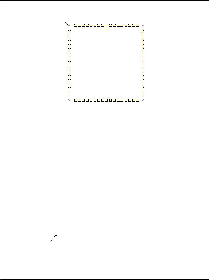
PN80-1 |
|
|
|
|
|
|
|
|
|
|
|
|
|
|
|
|
|
|
|
|
|
|
52 |
BIT OER |
||||||||||||||||
|
|
|
|
|
|
|
|
|
|
|
|
|
|
|
|
|
|
|
|
|
|
|
|
|
|
|
|
|
|
|
|
|
|
|
|
|
|
|
|
|
|
|
|
|
|
|||||||||||||||||||||
BIT OEL |
|
10 |
|
|
|
|
|
|
|
|
|
|
|
|
|
|
|
|
|
|
|
|
|
|
|
|
|
|
|
|
|
|
|
|
|
|
|
|
|
|
|
|
|
|
|
|
|
|
|
|
|
|
|
|
|
|
|
|
|
51 |
GND |
|||||
|
VCC |
|
|
11 |
|
|
|
|
|
|
|
|
|
|
|
|
|
|
|
|
|
|
|
80-Pin TQFP |
|
|
|
|
|
|
|
|
|
|
|
|
|
|
|
|
50 |
GND |
||||||||||||||||||||||||
|
|
|
|
|
|
|
|
|
|
|
|
|
|
|
|
|
|
|
|
|
|
|
|
|
|
|
|
|
|
|
|
|
|
|
|
|
|
|||||||||||||||||||||||||||||
BYTE R/WL |
|
|
12 |
|
|
|
|
|
|
|
|
|
|
|
|
|
|
|
|
|
|
|
|
|
|
|
|
|
|
|
|
|
|
|
|
|
|
|
49 |
BYTE R/WR |
||||||||||||||||||||||||||
BIT R/WL |
|
|
13 |
|
|
|
|
|
|
|
|
|
|
|
|
|
|
|
|
|
|
|
Top View (3) |
|
|
|
|
|
|
|
|
|
|
|
|
|
|
|
|
48 |
BIT R/WR |
|||||||||||||||||||||||||
|
|
|
|
|
|
|
|
|
|
|
|
|
|
|
|
|
|
|
|
|
|
|
|
|
|
|
|
|
|
|
|
|
|
|
|
|
||||||||||||||||||||||||||||||
|
N/C |
|
|
14 |
|
|
|
|
|
|
|
|
|
|
|
|
|
|
|
|
|
|
|
|
|
|
|
|
|
|
|
|
|
|
|
|
|
|
|
|
|
|
|
|
|
|
|
|
|
|
|
|
|
|
|
|
|
|
|
|
|
47 |
N/C |
|||
|
|
|
|
|
|
|
|
|
|
|
|
|
|
|
|
|
|
|
|
|
|
|
|
|
|
|
|
|
|
|
|
|
|
|
|
|
|
|
|
|
|
|
|
|
|
|
|
|
|
|
|
|
|
|
|
|
|
|
|
|||||||
|
CEL |
|
|
15 |
|
|
|
|
|
|
|
|
|
|
|
|
|
|
|
|
|
|
|
|
|
|
|
|
|
|
|
|
|
|
|
|
|
|
|
|
|
|
|
|
|
|
|
|
|
|
|
|
|
|
|
|
|
|
|
|
|
46 |
CER |
|||
|
|
|
|
|
|
|
|
|
|
|
|
|
|
|
|
|
|
|
|
|
|
|
|
|
|
|
|
|
|
|
|
|
|
|
|
|
|
|
|
|
|
|
|
|
|
|
|
|
|
|
|
|
|
|
|
|
|
|
|
|||||||
|
GND |
|
|
16 |
|
|
|
|
|
|
|
|
|
|
|
|
|
|
|
|
|
|
|
|
|
|
|
|
|
|
|
|
|
|
|
|
|
|
|
|
|
|
|
|
|
|
|
|
|
|
|
|
|
|
|
|
|
|
|
|
|
45 |
GND |
|||
|
|
|
|
|
|
|
|
|
|
|
|
|
|
|
|
|
|
|
|
|
|
|
|
|
|
|
|
|
|
|
|
|
|
|
|
|
|
|
|
|
|
|
|
|
|
|
|
|
|
|
|
|
|
|
|
|
|
|
|
|||||||
|
I/O8L |
|
|
17 |
|
|
|
|
|
|
|
|
|
|
|
|
|
|
|
|
|
|
|
|
|
|
|
|
|
|
|
|
|
|
|
|
|
|
|
|
|
|
|
|
|
|
|
|
|
|
|
|
|
|
|
|
|
|
|
|
|
44 |
I/O8R |
|||
|
I/O7L |
|
|
18 |
|
|
|
|
|
|
|
|
|
|
|
|
|
|
|
|
|
|
|
|
|
|
|
|
|
|
|
|
|
|
|
|
|
|
|
|
|
|
|
|
|
|
|
|
|
|
|
|
|
|
|
|
|
|
|
|
|
43 |
I/O7R |
|||
|
|
|
|
|
|
|
|
|
|
|
|
|
|
|
|
|
|
|
|
|
|
|
|
|
|
|
|
|
|
|
|
|
|
|
|
|
|
|
|
|
|
|
|
|
|
|
|
|
|
|
|
|
|
|
|
|
|
|
|
|||||||
|
I/O6L |
|
|
19 |
|
|
|
|
|
|
|
|
|
|
|
|
|
|
|
|
|
|
|
|
|
|
|
|
|
|
|
|
|
|
|
|
|
|
|
|
|
|
|
|
|
|
|
|
|
|
|
|
|
|
|
|
|
|
|
|
|
42 |
I/O6R |
|||
|
|
|
|
|
|
|
|
|
|
|
|
|
|
|
|
|
|
|
|
|
|
|
|
|
|
|
|
|
|
|
|
|
|
|
|
|
|
|
|
|
|
|
|
|
|
|
|
|
|
|
|
|
|
|
|
|
|
|
|
|||||||
|
N/C |
|
|
20 |
|
|
|
|
|
|
|
|
|
|
|
|
|
|
|
|
|
|
|
|
|
|
|
|
|
|
|
|
|
|
|
|
|
|
|
|
|
|
|
|
|
|
|
|
|
|
|
|
|
|
|
|
|
|
|
|
|
41 |
N/C |
|||
|
|
|
|
|
|
|
|
|
|
|
|
|
|
|
|
|
|
|
|
|
|
|
|
|
|
|
|
|
|
|
|
|
|
|
|
|
|
|
|
|
|
|
|
|
|
|
|
|
|
|
|
|
|
|
|
|
|
|
|
|||||||
|
|
|
|
|
21 |
22 |
23 |
24 |
25 |
26 |
27 |
28 |
29 |
30 |
31 |
32 |
33 |
34 |
35 |
36 |
37 |
38 |
39 |
40 |
|
|
||||||||||||||||||||||||||||||||||||||||
|
|
|
|
|
|
|
|
|
|
|
|
|
|
|
|
|
|
|
|
|
|
|
|
|
|
|
|
|
|
|
|
|
|
|
|
|
|
|
|
|
|
|
|
|
|
|
|
|
|
|
|
|
|
|
|
|
|
|
|
|
|
|
|
|
|
3007 drw 04 |
|
|
|
|
|
N/C |
N/C |
I/O5L |
VCC |
I/O4L |
I/O3L |
I/O2L |
I/O1L |
I/O0L |
GND |
GND |
I/O0R |
|
I/O1R |
|
I/O2R |
|
I/O3R |
|
VCC |
|
I/O4R |
|
I/O5R |
|
N/C |
|
N/C |
||||||||||||||||||||||||||||||||||
|
|
|
|
|
|
|
|
|
|
|
|
|
|
|||||||||||||||||||||||||||||||||||||||||||||||||||||
NOTES:
1.All VCC pins must be connected to power supply.
2.All ground pins must be connected to ground supply.
3.This text does not indicate the orientaion of the actual part-marking.
RECOMMENDED OPERATING
TEMPERATURE AND SUPPLY VOLTAGE
ABSOLUTE MAXIMUM RATINGS(1)
Symbol |
Rating |
Commercial |
Military |
Unit |
|
|
|
|
|
VTERM(2) |
Terminal Voltage |
–0.5 to +7.0 |
–0.5 to +7.0 |
V |
|
with Respect to |
|
|
|
|
GND |
|
|
|
|
|
|
|
|
VTERM(3) |
Terminal Voltage |
–0.5 to VCC |
–0.5 to VCC |
V |
TA |
Operating |
0 to +70 |
–55 to +125 |
°C |
|
Temperature |
|
|
|
|
|
|
|
|
TBIAS |
Temperature |
–55 to +125 |
–65 to +135 |
°C |
|
Under Bias |
|
|
|
|
|
|
|
|
TSTG |
Storage |
–55 to +125 |
–65 to +150 |
°C |
|
Temperature |
|
|
|
|
|
|
|
|
IOUT |
DC Output Current |
50 |
50 |
mA |
NOTES: |
|
|
3007 tbl 01 |
|
|
Ambient |
|
|
Grade |
Temperature |
GND |
VCC |
|
|
|
|
Military |
–55°C to +125°C |
0V |
5.0V ± 10% |
Commercial |
0°C to +70°C |
0V |
5.0V ± 10% |
|
|
|
|
|
|
|
3007 tbl 02 |
RECOMMENDED DC OPERATING |
|
||
CONDITIONS |
|
|
|
Symbol |
Parameter |
Min. |
Typ. |
Max. |
Unit |
VCC |
Supply Voltage |
4.5 |
5.0 |
5.5 |
V |
GND |
Supply Voltage |
0 |
0 |
0 |
V |
VIH |
Input High Voltage |
2.2 |
— |
6.0 (2) |
V |
VIL |
Input Low Voltage |
–0.5(1) |
— |
0.8 |
V |
NOTES: |
|
|
|
|
3007 tbl 03 |
1.VIL > -1.5V for pulse width less than 10ns.
2.VTERM must not exceed Vcc + 0.5V.
CAPACITANCE(1)
(TA = +25°C, F = 1.0MHZ) TQFP ONLY
1.Stresses greater than those listed under ABSOLUTE MAXIMUM RATINGS may cause permanent damage to the device. This is a stress rating only and functional operation of the device at these or any other conditions above those indicated in the operational sections of this specification is not implied. Exposure to absolute maximum rating conditions for extended periods may affect reliability.
2.VTERM must not exceed Vcc + 0.5V for more than 25% of the cycle time or 10ns maximum, and is limited to < 20mA for the period of VTERM > Vcc + 0.5V.
Symbol |
Parameter |
Condition(2) |
Max. |
Unit |
CIN |
Input Capacitance |
VIN = 3dV |
9 |
pF |
|
|
|
|
|
COUT |
Output Capacitance |
VOUT = 3dV |
10 |
pF |
|
|
|
|
|
NOTES:
1.These parameters are determined by device characterization, but are not production tested.
2.3dV references the interpolated capacitance when the input and output switch from 0V to 3V or from 3V to 0V.
6.23 |
3 |
 Loading...