


Integrated Device Technology Inc IDT49C460AFF, IDT49C460AFFB, IDT49C460AG, IDT49C460CG, IDT49C460CGB Datasheet
...Integrated Device Technology, Inc.
|
IDT49C460 |
32-BIT CMOS |
IDT49C460A |
ERROR DETECTION |
IDT49C460B |
IDT49C460C |
|
AND CORRECTION UNIT |
IDT49C460D |
|
IDT49C460E |
FEATURES:
• Fast |
|
|
|
Detect |
Correct |
— IDT49C460E |
10ns (max.) |
14ns (max.) |
— IDT49C460D |
12ns (max.) |
18ns (max.) |
— IDT49C460C |
16ns (max.) |
24ns (max.) |
— IDT49C460B |
25ns (max.) |
30ns (max.) |
— IDT49C460A |
30ns (max.) |
36ns (max.) |
— IDT49C460 |
40ns (max.) |
49ns (max.) |
•Low-power CMOS
—Commercial: 95mA (max.)
—Military: 125mA (max.)
•Improves system memory reliability
—Corrects all single bit errors, detects all double and some triple-bit errors
•Cascadable
—Data words up to 64-bits
•Built-in diagnostics
—Capable of verifying proper EDC operation via software control
•Simplified byte operations
—Fast byte writes possible with separate byte enables
•Functional replacement for 32and 64-bit configurations of the AM29C60 and AM29C660
•Available in PGA, PLCC and Fine Pitch Flatpack
•Military product compliant to MIL-STD-883, Class B
•Standard Military Drawing #5962–88533
DESCRIPTION:
The IDT49C460s are high-speed, low-power, 32-bit Error Detection and Correction Units which generate check bits on a 32-bit data field according to a modified Hamming Code and correct the data word when check bits are supplied. The IDT49C460s are performance-enhanced functional replacements for 32-bit versions of the 2960. When performing a read operation from memory, the IDT49C460s will correct 100% of all single bit errors and will detect all double bit errors and some triple bit errors.
The IDT49C460s are easily cascadable to 64-bits. Thirty- two-bit systems use 7 check bits and 64-bit systems use 8 check bits. For both configurations, the error syndrome is made available.
The IDT49C460s incorporate two built-in diagnostic modes. Both simplify testing by allowing for diagnostic data to be entered into the device and to execute system diagnostics functions.
They are fabricated using a CMOS technology designed for high-performance and high-reliability. The devices are packaged in a 68-pin ceramic PGA, PLCC and Ceramic Quad Flatpack.
Military grade product is manufactured in compliance with the latest revision of MIL-STD-883, Class B, making it ideally suited to military temperature applications demanding the highest level of performance and reliability.
FUNCTIONAL BLOCK DIAGRAM
CB0–7
|
|
8 |
|
|
|
|
|
|
|
|
|
|
|
|
|
|
|
|
|
|
|
|
|
|
|
|
DATA0–31 |
|
|
DATA |
|
|
|
|
ERROR |
|
|
|
|
ERROR |
|
MUX |
|
|
|
|
|
|
|||
|
|
|
|
|
|
|
|
|
|
|
|
|
|
|
|
|
|
||||||||
|
|
|
|
LATCH |
|
32 |
|
CORRECT |
|
|
|
DECODE |
8 |
|
|
|
|
|
|
||||||
|
|
|
|
|
|
|
|
|
|
|
|
|
|
|
|
||||||||||
|
|
|
|
|
|
|
|
|
|
|
|
|
|
|
|
|
|
|
|
|
|
|
|||
|
OE BYTE0–3 |
4 |
|
|
|
|
|
|
|
|
|
|
|
|
|
|
|
|
|
|
|
|
|
|
|
|
|
|
|
|
|
|
|
|
|
|
|
|
|
|
|
|
8 |
|
|
|
|
||||
|
|
|
|
|
|
|
|
|
32 |
|
|
|
|
|
|
|
|
|
|
|
|
|
|||
|
|
|
|
|
|
|
|
|
|
|
|
|
|
|
|
|
|
|
|
|
|
|
|
||
|
|
|
|
DATA |
|
|
|
|
|
CHECK BIT |
|
|
|
|
|
|
|
|
|
SC0–7 |
|||||
|
|
|
|
|
|
|
|
|
|
|
|
|
|
|
|
|
|
||||||||
|
|
32 |
LATCH |
|
|
|
|
|
GENERATE |
|
|
8 |
|
|
|
|
|
|
|||||||
|
|
|
|
|
|
|
|
|
|
|
|
|
|
|
|
||||||||||
|
|
|
|
|
|
|
|
|
|
|
|
|
|
|
|
|
|
|
|
|
|
|
MUX |
|
OESC |
|
|
|
|
|
|
|
|
|
|
MUX |
8 |
|
|
|
|
||||||||||
|
|
|
|
|
|
|
|
|
|
|
|
|
|
|
|
|
|
|
|
||||||
|
|
|
|
CHECK BIT |
|
|
|
|
|
|
|
|
|
|
|
|
|
|
|
|
|||||
|
|
|
|
|
|
|
|
|
|
|
|
|
|
|
|
|
|
|
|
|
|
|
|
||
|
LEIN |
|
|
IN LATCH |
|
|
|
|
|
|
|
|
|
|
|
|
|
|
|
|
|
|
|
ERROR |
|
|
|
|
|
|
|
|
|
|
|
|
|
|
|
|
|
|
|
|
|
|
|
||||
|
|
|
|
|
|
|
|
|
|
|
|
|
|
|
|
|
|
|
|
|
|
|
|
||
|
|
|
|
|
|
|
|
|
|
|
|
|
|
|
|
|
|
|
|
|
|
|
|
||
|
|
|
|
|
|
|
|
|
|
|
|
|
|
MUX |
|
SYNDROME |
|
|
|
ERROR |
|||||
|
|
|
|
|
|
|
|
|
|
|
|
|
|
|
|
|
|
|
|||||||
|
|
|
|
|
|
|
|
|
|
|
|
|
|
|
|
|
|
|
|
||||||
|
|
13 |
|
|
|
|
|
|
|
|
|
|
|
|
GENERATE |
|
|
|
DETECT |
MULT ERROR |
|||||
|
|
DIAGNOSTIC |
|
|
|
|
|
|
|
|
|
|
|
|
|
|
|
||||||||
|
|
|
|
|
|
|
|
|
|
|
|
|
|
|
|
|
|
|
|
|
|
|
|
||
|
|
|
|
|
|
|
|
|
|
|
|
|
|
|
|
|
|
|
|
|
|
|
|
||
|
|
|
|
LATCH |
|
|
|
|
|
|
|
|
|
|
|
|
|
|
|
|
|
|
|
|
|
|
LEDIAG |
|
|
|
|
|
|
|
|
|
|
8 |
|
|
|
|
|
|
|
|
|
|
|
|
|
|
|
|
|
|
5 |
|
|
|
|
|
|
|
|
|
|
|
|
|
|
|
|
|
|||
|
|
|
|
|
|
|
|
|
|
|
|
|
|
|
|
|
|
|
|
|
|
|
|
||
LEOUT/GENERATE |
|
|
|
|
|
|
|
|
|
|
|
|
|
|
|
|
|
|
|
|
|
|
|
|
|
|
|
|
|
|
|
|
|
|
|
|
|
|
|
|
|
|
|
|
|
|
|
|
|
||
|
CORRECT |
|
|
CONTROL |
|
|
|
|
|
|
|
|
|
|
|
|
|
|
|
|
|
|
|
|
|
|
CODE ID1,0 |
|
|
LOGIC |
|
|
|
|
|
|
|
|
|
|
|
|
|
|
|
|
|
|
|
|
|
|
DIAG MODE1,0 |
|
|
|
|
|
|
|
|
|
|
|
|
|
|
|
|
|
|
|
|
|
|
|
|
|
The IDT logo is a registered trademark of Integrated Device Technology, Inc. |
|
|
|
|
|
|
|
|
|
|
|
|
|
|
|
|
2584 drw 01 |
|||||||
|
MILITARY AND COMMERCIAL TEMPERATURE RANGES |
|
|
|
|
|
|
|
|
|
AUGUST 1995 |
||||||||||||||
|
|
|
|
|
|
|
|
|
|
|
|
|
|
|
|
|
|
|
|
|
|
|
|
|
|
|
©1995 Integrated Device Technology, Inc. |
|
|
|
|
|
|
|
|
11.6 |
|
|
|
|
|
|
|
|
|
DSC-9017/8 |
|||||
1

IDT49C460/A/B/C/D/E |
|
32-BIT CMOS ERROR DETECTION AND CORRECTION UNIT |
MILITARY AND COMMERCIAL TEMPERATURE RANGES |
PIN CONFIGURATIONS
VCC 10
D2 11
D3 12
D4 13
D5 14
D6 15
D7 16
D8 17
GND 18
D9 19
D10 20
D11 21
D12 22
D13 23
D14 24
D15 25
OE1 26
D1 |
D0 OE 0 |
LEIN |
DIAG MODE1 |
DIAG MODE0 |
CODE ID1 |
CODE ID0 |
OE3 |
D31 D30 D29 D28 D27 D26 D25 GND |
|
9 |
8 |
7 |
6 |
5 |
4 |
3 |
2 |
1 68 67 66 65 64 63 62 61 |
|
J68–1
27 28 29 30 31 32 33 34 35 36 37 38 39 40 41 42 43
CB7 |
CB6 |
CB5 |
CB4 |
CB3 |
CB2 |
CB1 |
CB0 |
SC0 |
SC1 |
SC2 |
SC3 |
SC4 |
SC5 |
SC6 |
SC7 OESC |
PLCC
TOPVIEW
DESIGNATES
PIN 1 FOR
PLCC ONLY
60 |
D24 |
59 |
D23 |
58 |
D22 |
57 |
D21 |
56 |
D20 |
55 |
D19 |
54 |
D18 |
53 |
D17 |
52 |
VCC |
51 |
D16 |
50 |
OE2 |
49 |
LEOUT/GENERATE |
48 |
CORRECT |
47 |
LEDIAG |
46 |
ERROR |
45 |
MULT ERROR |
44 |
GND |
2584 drw 02
11.6 |
2 |

IDT49C460/A/B/C/D/E |
|
32-BIT CMOS ERROR DETECTION AND CORRECTION UNIT |
MILITARY AND COMMERCIAL TEMPERATURE RANGES |
D1 |
D0 OE0 |
LEIN |
DIAG MODE1 |
DIAG MODE0 CODE ID1 |
CODE ID0 OE3 |
D31 |
D30 |
D29 |
D28 |
D27 |
D26 |
D25 |
GND |
|
|
|
|
|
|
|
|
|
|
|
|
|
|
|
|
|
|
|
|
|
|
|
|
|
|
|
|
|
|
|
|
|
|
|
|
|
|
|
|
|
|
|
|
|
|
|
|
|
|
|
|
|
|
|
|
|
|
|
|
|
|
|
|
|
|
|
|
|
|
|
|
|
|
|
|
|
|
|
|
|
|
|
|
|
|
|
|
|
|
|
|
|
|
|
|
|
|
|
|
|
9 |
|
8 |
|
7 |
|
6 |
|
5 |
|
4 |
|
3 |
|
2 |
|
1 |
|
68 67 66 65 64 63 62 61 |
|
|
|
|
|
D24 |
||||||||||||||||||
|
|
|
|
|
|
|
|
|
|
|
|
|
|
|
|
|
|
||||||||||||||||||||||||||||||
|
|
|
|
|
|
|
|||||||||||||||||||||||||||||||||||||||||
VCC |
|
|
10 |
|
|
|
|
|
|
|
|
|
|
|
|
|
|
|
|
|
|
|
|
|
|
|
|
|
|
|
|
|
|
|
|
60 |
|
|
|
|
|||||||
|
|
|
|
|
|
|
|
|
|
|
|
|
|
|
|
|
|
|
|
|
|
|
|
|
|
|
|
|
|
|
|
|
|
|
|||||||||||||
|
|
|
|
|
|
|
|
|
|
|
|
|
|
|
|
|
|
|
|
|
|
|
|
|
|
|
|
|
|
|
|
|
|
|
|||||||||||||
D2 |
|
|
11 |
|
|
|
|
|
|
|
|
|
|
|
|
|
|
|
|
|
|
|
|
|
|
|
|
|
|
|
|
|
|
|
|
59 |
|
|
|
|
D23 |
||||||
|
|
|
|
|
|
|
|
|
|
|
|
|
|
|
|
|
|
|
|
|
|
|
|
|
|
|
|
|
|
|
|
|
|
|
|||||||||||||
|
|
|
|
|
|
|
|
|
|
|
|
|
|
|
|
|
|
|
|
|
|
|
|
|
|
|
|
|
|
|
|
|
|
|
|||||||||||||
D3 |
|
|
12 |
|
|
|
|
|
|
|
|
|
|
|
|
|
|
|
|
|
|
|
|
|
|
|
|
|
|
|
|
|
|
|
|
58 |
|
|
|
|
D22 |
||||||
|
|
|
|
|
|
|
|
|
|
|
|
|
|
|
|
|
|
|
|
|
|
|
|
|
|
|
|
|
|
|
|
|
|
|
|||||||||||||
|
|
|
|
|
|
|
|
|
|
|
|
|
|
|
|
|
|
|
|
|
|
|
|
|
|
|
|
|
|
|
|
|
|
|
|||||||||||||
D4 |
|
|
13 |
|
|
|
|
|
|
|
|
|
|
PIN 1 IDENTIFICATION |
57 |
|
|
|
|
D21 |
|||||||||||||||||||||||||||
|
|
|
|
|
|
|
|
|
|
|
|
||||||||||||||||||||||||||||||||||||
|
|
|
|
|
|
|
|
|
|
|
|
||||||||||||||||||||||||||||||||||||
D5 |
|
|
14 |
|
|
|
|
|
|
|
|
|
|
|
|
|
|
|
|
|
|
|
|
|
|
|
|
|
|
|
|
|
|
|
|
56 |
|
|
|
|
D20 |
||||||
|
|
|
|
|
|
|
|
|
|
|
|
|
|
|
|
|
|
|
|
|
|
|
|
|
|
|
|
|
|
|
|
|
|
|
|||||||||||||
|
|
|
|
|
|
|
|
|
|
|
|
|
|
|
|
|
|
|
|
|
|
|
|
|
|
|
|
|
|
|
|
|
|
|
|||||||||||||
D6 |
|
|
15 |
|
|
|
|
|
|
|
|
|
|
|
|
|
|
|
|
|
|
|
|
|
|
|
|
|
|
|
|
|
|
|
|
55 |
|
|
|
|
D19 |
||||||
|
|
|
|
|
|
|
|
|
|
|
|
|
|
|
|
|
|
|
|
|
|
|
|
|
|
|
|
|
|
|
|
|
|
|
|||||||||||||
|
|
|
|
|
|
|
|
|
|
|
|
|
|
|
|
|
|
|
|
|
|
|
|
|
|
|
|
|
|
|
|
|
|
|
|||||||||||||
D7 |
|
|
16 |
|
|
|
|
|
|
|
|
|
|
|
|
|
|
|
|
|
|
|
|
|
|
|
|
|
|
|
|
|
|
|
|
54 |
|
|
|
|
D18 |
||||||
|
|
|
|
|
|
|
|
|
|
|
|
|
|
|
|
|
|
|
|
|
|
|
|
|
|
|
|
|
|
|
|
|
|
|
|||||||||||||
|
|
|
|
|
|
|
|
|
|
|
|
|
|
|
|
|
|
|
|
|
|
|
|
|
|
|
|
|
|
|
|
|
|
|
|||||||||||||
D8 |
|
|
17 |
|
|
|
|
|
|
|
|
|
|
|
|
|
|
|
F68 - 2 |
53 |
|
|
|
|
D17 |
||||||||||||||||||||||
|
|
|
|
|
|
|
|
|
|
|
|
|
|
|
|
|
|
||||||||||||||||||||||||||||||
|
|
|
|
|
|
|
|
|
|
|
|
|
|
|
|
|
|
||||||||||||||||||||||||||||||
GND |
|
|
18 |
|
|
|
|
|
|
|
|
|
|
|
|
|
|
|
52 |
|
|
|
|
VCC |
|||||||||||||||||||||||
|
|
|
|
|
|
|
|
|
|
|
|
|
|
|
|
|
|
|
|
|
|||||||||||||||||||||||||||
|
|
|
|
|
|
|
|
|
|
|
|
|
|
|
|
|
|
|
|
|
|
|
|
|
|
|
|
|
|
|
|
|
|
|
|
|
|
||||||||||
D9 |
|
|
19 |
|
|
|
|
|
|
|
|
|
|
|
|
|
|
|
|
|
|
|
|
|
|
|
|
|
|
|
|
|
|
|
|
51 |
|
|
|
|
D16 |
||||||
|
|
|
|
|
|
|
|
|
|
|
|
|
|
|
|
|
|
|
|
|
|
|
|
|
|
|
|
|
|
|
|
|
|
|
|||||||||||||
|
|
|
|
|
|
|
|
|
|
|
|
|
|
|
|
|
|
|
|
|
|
|
|
|
|
|
|
|
|
|
|
|
|
|
|||||||||||||
D10 |
|
|
20 |
|
|
|
|
|
|
|
|
|
|
|
|
|
|
|
|
|
|
|
|
|
|
|
|
|
|
|
|
|
|
|
|
50 |
|
|
|
|
OE2 |
||||||
|
|
|
|
|
|
|
|
|
|
|
|
|
|
|
|
|
|
|
|
|
|
|
|
|
|
|
|
|
|
|
|
|
|
|
|||||||||||||
|
|
|
|
|
|
|
|
|
|
|
|
|
|
|
|
|
|
|
|
|
|
|
|
|
|
|
|
|
|
|
|
|
|
|
|||||||||||||
D11 |
|
|
21 |
|
|
|
|
|
|
|
|
|
|
|
|
|
|
|
|
|
|
|
|
|
|
|
|
|
|
|
|
|
|
|
|
49 |
|
|
|
|
LEOUT/GENERATE |
||||||
|
|
|
|
|
|
|
|
|
|
|
|
|
|
|
|
|
|
|
|
|
|
|
|
|
|
|
|
|
|
|
|
|
|
|
|||||||||||||
|
|
|
|
|
|
|
|
|
|
|
|
|
|
|
|
|
|
|
|
|
|
|
|
|
|
|
|
|
|
|
|
|
|
|
|||||||||||||
D12 |
|
|
22 |
|
|
|
|
|
|
|
|
|
|
|
|
|
|
|
|
|
|
|
|
|
|
|
|
|
|
|
|
|
|
|
|
48 |
|
|
|
|
CORRECT |
||||||
|
|
|
|
|
|
|
|
|
|
|
|
|
|
|
|
|
|
|
|
|
|
|
|
|
|
|
|
|
|
|
|
|
|
|
|||||||||||||
|
|
|
|
|
|
|
|
|
|
|
|
|
|
|
|
|
|
|
|
|
|
|
|
|
|
|
|
|
|
|
|
|
|
|
|||||||||||||
D13 |
|
|
23 |
|
|
|
|
|
|
|
|
|
|
|
|
|
|
|
|
|
|
|
|
|
|
|
|
|
|
|
|
|
|
|
|
47 |
|
|
|
|
LEDIAG |
||||||
|
|
|
|
|
|
|
|
|
|
|
|
|
|
|
|
|
|
|
|
|
|
|
|
|
|
|
|
|
|
|
|
|
|
|
|||||||||||||
|
|
|
|
|
|
|
|
|
|
|
|
|
|
|
|
|
|
|
|
|
|
|
|
|
|
|
|
|
|
|
|
|
|
|
|||||||||||||
D14 |
|
|
24 |
|
|
|
|
|
|
|
|
|
|
|
|
|
|
|
|
|
|
|
|
|
|
|
|
|
|
|
|
|
|
|
|
46 |
|
|
|
|
ERROR |
||||||
|
|
|
|
|
|
|
|
|
|
|
|
|
|
|
|
|
|
|
|
|
|
|
|
|
|
|
|
|
|
|
|
|
|
|
|||||||||||||
|
|
|
|
|
|
|
|
|
|
|
|
|
|
|
|
|
|
|
|
|
|
|
|
|
|
|
|
|
|
|
|
|
|
|
MULT ERROR |
||||||||||||
D15 |
|
|
25 |
|
|
|
|
|
|
|
|
|
|
|
|
|
|
|
|
|
|
|
|
|
|
|
|
|
|
|
|
|
|
|
|
45 |
|
|
|
|
|||||||
|
|
|
|
|
|
|
|
|
|
|
|
|
|
|
|
|
|
|
|
|
|
|
|
|
|
|
|
|
|
|
|
|
|
|
|||||||||||||
|
|
|
|
|
|
|
|
|
|
|
|
|
|
|
|
|
|
|
|
|
|
|
|
|
|
|
|
|
|
|
|
|
|
|
GND |
||||||||||||
OE1 |
|
|
26 |
|
|
|
|
|
|
|
|
|
|
|
|
|
|
|
|
|
|
|
|
|
|
|
|
|
|
|
|
|
|
|
|
44 |
|
|
|
|
|||||||
|
|
|
|
|
|
|
|
|
|
|
|
|
|
|
|
|
|
|
|
|
|
|
|
|
|
|
|
|
|
|
|
|
|
|
|||||||||||||
|
|
|
|
|
|
|
|
|
|
|
|
|
|
|
|
|
|
|
|
|
|
|
|
|
|
|
|
|
|
|
|
|
|
|
|||||||||||||
|
|
|
|
27 28 29 30 31 32 33 34 35 36 37 38 39 40 41 42 43 |
|
|
|
|
2584 drw 03 |
||||||||||||||||||||||||||||||||||||||
|
|
|
|
|
|
|
|
||||||||||||||||||||||||||||||||||||||||
|
|
|
|
|
|
|
|
|
|
|
|
|
|
|
|
|
|
|
|
|
|
|
|
|
|
|
|
|
|
|
|
|
|
|
|
|
|
|
|
|
|
|
|
|
|
||
|
|
|
|
|
|
|
|
|
|
|
|
|
|
|
|
|
|
|
|
|
|
|
|
|
|
|
|
|
|
|
|
|
|
|
|
|
|
|
|
|
|
|
|
|
|
||
|
|
|
|
|
|
|
|
|
|
|
|
|
|
|
|
|
|
|
|
|
|
|
|
|
|
|
|
|
|
|
|
|
|
|
|
|
|
|
|
|
|
|
|
|
|
|
|
|
|
|
|
|
|
CB7 |
|
CB6 |
CB5 |
CB4 |
CB3 |
CB2 |
CB1 |
CB0 |
SC0 |
|
SC1 SC2 SC3 SC4 SC5 SC6 |
SC7 OESC |
|
|
|
|
|||||||||||||||||||||||||
FINE PITCH FLATPACK
TOPVIEW
11.6 |
3 |
IDT49C460/A/B/C/D/E |
|
32-BIT CMOS ERROR DETECTION AND CORRECTION UNIT |
MILITARY AND COMMERCIAL TEMPERATURE RANGES |
D25
D27
D26
D29
D28
D31
D30
CODE ID0
OE3
DIAG MODE0
CODE ID1
LEIN
DIAG MODE1 D0
OE 0
D1
D24 |
GND D23 |
D22 |
D21 |
D20 |
D19 |
D18 |
D17 |
VCC |
D16 OE2 LEOUT/GENERATE |
CORRECT LEDIAG ERROR MULTERROR |
GND |
||||||||||||
|
|
|
|
|
|
|
|
|
|
|
|
|
|
|
|
|
|
|
|
|
|
|
|
|
|
|
|
|
|
|
|
|
|
|
|
|
|
|
|
|
|
|
|
|
|
|
|
53 |
51 |
|
50 |
|
48 |
|
46 |
44 |
|
42 |
|
40 |
|
38 |
|
36 |
34 |
|
||||||||||||||||||||||
|
|
|
|
|
|
|
|
|
|
|
|
|
|
|
|
|
|
|
|
|
|
|
|
|
|
|
|
|
|
|
|
|
|
|
||||||
|
|
|
|
|
|
|
|
|
|
|
|
|
|
|
|
|
|
|
|
|
|
|
|
|
|
|
|
|
|
|
|
|
|
|
|
|
|
|
|
|
|
|
|
52 |
|
49 |
|
47 |
|
45 |
43 |
|
41 |
|
39 |
|
37 |
|
35 |
|
|
|
OESC |
||||||||||||||||||
|
|
55 |
|
|
|
54 |
|
|
|
|
|
|
|
|
|
|
|
|
|
|
|
|
|
|
|
|
|
|
|
|
|
|
32 |
|
|
33 |
|
|
|
SC7 |
|
|
|
|
|
|
|
|
|
|
|
|
|
|
|
|
|
|
|
|
|
|
|
|
|
|
|
|
|
|
|
|
|
|
|||||||
|
|
|
|
|
|
|
|
|
|
|
|
|
|
|
|
|
|
|
|
|
|
|
|
|
|
|
|
|
|
|
|
|
|
|||||||
|
|
|
|
|
|
|
|
|
|
|
|
|
|
|
|
|
|
|
|
|
|
|
|
|
|
|
|
|
|
|
|
|
|
|
|
|
|
|
|
SC6 |
|
|
57 |
|
|
|
56 |
|
|
|
|
|
|
|
|
|
|
|
|
|
|
|
|
|
|
|
|
|
|
|
|
|
|
30 |
|
|
31 |
|
|
|
SC5 |
|
|
|
|
|
|
|
|
|
|
|
|
|
|
|
|
|
|
|
|
|
|
|
|
|
|
|
|
|
|
|
|
|
|
|||||||
|
|
|
|
|
|
|
|
|
|
|
|
|
|
|
|
|
|
|
|
|
|
|
|
|
|
|
|
|
|
|
|
|
|
|||||||
|
|
|
|
|
|
|
|
|
|
|
|
|
|
|
|
|
|
|
|
|
|
|
|
|
|
|
|
|
|
|
|
|
|
|
|
|
|
|
|
SC4 |
|
|
59 |
|
|
|
58 |
|
|
|
|
|
|
|
|
|
|
|
|
|
|
|
|
|
|
|
|
|
|
|
|
|
|
28 |
|
|
29 |
|
|
|
SC3 |
|
|
|
|
|
|
|
|
|
|
|
|
|
|
|
|
|
|
|
|
|
|
|
|
|
|
|
|
|
|
|
|
|
|
|||||||
|
|
|
|
|
|
|
|
|
|
|
|
|
|
|
|
|
|
|
|
|
|
|
|
|
|
|
|
|
|
|
|
|
|
|||||||
|
|
|
|
|
|
|
|
|
|
|
|
|
|
|
|
|
|
|
|
|
|
|
|
|
|
|
|
|
|
|
|
|
|
|
|
|
|
|
|
SC2 |
|
|
61 |
|
|
|
60 |
|
|
|
|
|
|
|
|
|
|
|
G68 – 1 |
|
|
|
|
|
|
|
|
|
|
|
26 |
|
|
27 |
|
|
|
SC1 |
|||
|
|
|
|
|
|
|
|
|
|
|
|
|
|
|
|
|
|
|
|
|
|
|
|
|
|
|
|
|
|
|||||||||||
|
|
|
|
|
|
|
|
|
|
|
|
|
|
|
|
|
|
|
|
|
|
|
|
|
|
|
|
|
|
|||||||||||
|
|
|
|
|
|
|
|
|
|
|
|
|
|
|
|
|
|
|
|
|
|
|
|
|
|
|
|
|
|
|
|
|
|
|
|
|
|
|
|
SC0 |
|
|
63 |
|
|
|
62 |
|
|
|
|
|
|
|
|
|
|
|
|
|
|
|
|
|
|
|
|
|
|
|
|
|
|
24 |
|
|
25 |
|
|
|
CB0 |
|
|
|
|
|
|
|
|
|
|
|
|
|
|
|
|
|
|
|
|
|
|
|
|
|
|
|
|
|
|
|
|
|
|
|||||||
|
|
|
|
|
|
|
|
|
|
|
|
|
|
|
|
|
|
|
|
|
|
|
|
|
|
|
|
|
|
|
|
|
|
|||||||
|
|
|
|
|
|
|
|
|
|
|
|
|
|
|
|
|
|
|
|
|
|
|
|
|
|
|
|
|
|
|
|
|
|
|
|
|
|
|
|
CB1 |
|
|
65 |
|
|
|
64 |
|
|
|
|
|
|
|
|
|
|
|
|
|
|
|
|
|
|
|
|
|
|
|
|
|
|
22 |
|
|
23 |
|
|
|
CB2 |
|
|
|
|
|
|
|
|
|
|
|
|
|
|
|
|
|
|
|
|
|
|
|
|
|
|
|
|
|
|
|
|
|
|
|||||||
|
|
|
|
|
|
|
|
|
|
|
|
|
|
|
|
|
|
|
|
|
|
|
|
|
|
|
|
|
|
|
|
|
|
|||||||
|
|
|
|
|
|
|
|
|
|
|
|
|
|
|
|
|
|
|
|
|
|
|
|
|
|
|
|
|
|
|
|
|
|
|
|
|
|
|
|
CB3 |
|
|
67 |
|
|
|
66 |
|
|
|
|
|
|
|
|
|
|
|
|
|
|
|
|
|
|
|
|
|
|
|
|
|
|
20 |
|
|
21 |
|
|
|
CB4 |
|
|
|
|
|
|
|
|
|
|
|
|
|
|
|
|
|
|
|
|
|
|
|
|
|
|
|
|
|
|
|
|
|
|
|||||||
|
|
|
|
|
|
|
|
|
|
|
|
|
|
|
|
|
|
|
|
|
|
|
|
|
|
|
|
|
|
|
|
|
|
|||||||
|
|
|
1 |
|
3 |
|
5 |
|
7 |
9 |
|
11 |
|
13 |
|
15 |
|
18 |
|
|
|
CB5 |
||||||||||||||||||
|
|
|
|
|
|
|
|
|
|
|
|
|
CB6 |
|||||||||||||||||||||||||||
|
|
|
|
|
|
|
|
|
|
|
|
|
|
|
|
|
|
|
|
|
|
|
|
|
|
|
|
|
|
|
|
|
|
|
|
|
|
|
|
|
68 |
2 |
|
4 |
|
6 |
|
8 |
10 |
|
12 |
|
14 |
|
16 |
|
17 |
19 |
|
||||||||||||||||||||||
|
|
|
|
|
|
|
|
|
|
|
|
|
|
|||||||||||||||||||||||||||
|
|
|
|
|
|
|
|
|
|
|
|
|
|
|
|
|
|
|
|
|
|
|
|
|
|
|
|
|
|
|
|
|
|
|
|
|
|
|
|
2584 drw 04 |
|
|
|
|
|
|
|
|
|
|
|
|
|
|
|
|
|
|
|
|
|
|
|
|
|
|
|
|
|
|
|
|
|
|
|
|
|
|
|
|
|
|
|
VCC |
|
D2 |
D3 |
|
D4 |
D5 |
|
D6 |
D7 |
|
D8 |
GND D9 |
D10 |
|
D11 |
D12 |
|
D13 |
D14 |
|
D15 |
CB7 |
OE 1 |
|
|
|
||||||||||||
|
|
|
|
|
|
|
|
|
|
|
|
|
||||||||||||||||||||||||||||
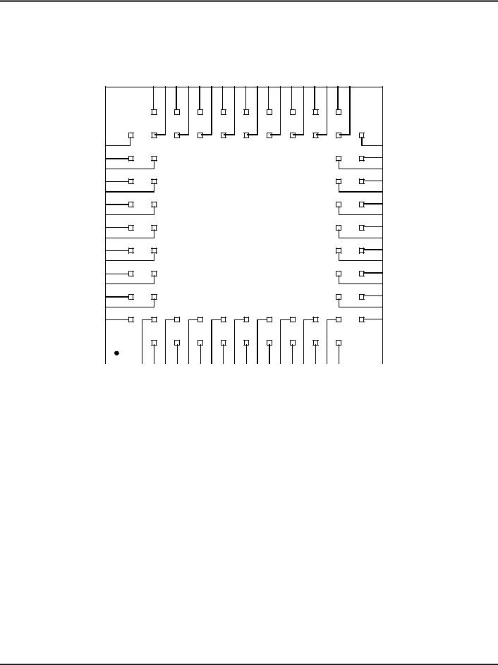
PGA
TOPVIEW
11.6 |
4 |

IDT49C460/A/B/C/D/E |
|
32-BIT CMOS ERROR DETECTION AND CORRECTION UNIT |
MILITARY AND COMMERCIAL TEMPERATURE RANGES |
PIN DESCRIPTIONS
Pin Name |
I/O |
Description |
DATA0–31 |
I/O |
32 bidirectional data lines provide input to the Data Input Latch and Diagnostic Latch and also receive output from |
|
|
the Data Output Latch. DATA0 is the LSB; DATA31 is the MSB. |
CB0–7 |
I |
Eight check bit input lines input check bits for error detection and also used to input syndrome bits for error |
|
|
correction in 64-bit applications. |
LEIN |
I |
Latch Enable is for the Data Input Latch. Controls latching of the input data. Data Input Latch and Check Bit Input |
|
|
Latch are latched to their previous state when LOW. When HIGH, the Data Input Latch and Check Bit Input Latch |
|
|
follow the input data and input check bits. |
LEOUT/
GENERATE
SC0–7
A multifunction pin which, when LOW, is in the Check Bit Generate Mode. In this mode, the device generates the check bits or GENERATE partial check bits specific to the data in the Data Input Latch. The generated check bits are placed on the SC outputs. Also, when LOW, the Data Out Latch is latched to its previous state.
When HIGH, the device is in the Detect or Correct Mode. In this mode, the device detects single and multiple errors and generates syndrome bits based upon the contents of the Data Input Latch and Check Bit Input Latch. In the Correct Mode, single bit errors are also automatically corrected and the corrected data is placed at the inputs of the Data Output Latch. The syndrome result is placed on the SC outputs and indicates in a coded form the number of errors and the specific bit-in-error. When HIGH, the Data Output Latch follows the output of the Data Input Latch as modified by the correction logic network. In Correct Mode, single bit errors are corrected by the network before being loaded into the Data Output Latch. In Detect Mode, the contents of the Data Input Latch are passed through the correction network unchanged into the Data Output Latch. The Data Output Latch is disabled, with its contents unchanged, if the EDC is in the Generate Mode.
OSyndrome Check Bit outputs. Eight outputs which hold the check bits and partial check bits when the EDC is in the Generate Mode and will hold the syndrome/partial syndrome bits when the device is in the Detect or Correct modes. All are 3-state outputs.
OESC |
I |
Output Enable—Syndrome Check Bits. In the HIGH condition, the SC outputs are in the high impedance state. |
|
|
When LOW, all SC output lines are enabled. |
ERROR |
O |
In the Detect or Correct Mode, this output will go LOW if one or more data or check bits contain an error. When |
|
|
HIGH, no errors have been detected. This pin is forced HIGH in the Generate Mode. |
MULT |
O |
In the Detect or Correct Mode, this output will go LOW if two or more bit errors have been detected. A HIGH level |
ERROR |
|
indicates that either one or no errors have been detected. This pin is forced HIGH in the Generate Mode. |
CORRECT |
I |
The correct input which, when HIGH, allows the correction network to correct any single-bit error in the Data Input |
|
|
Latch (by complementing the bit-in-error) before putting it into the Data Output Latch. When LOW, the device will |
|
|
drive data directly from the Data Input Latch to the Data Output Latch without correction. |
OE BYTE0–3 |
I |
Output Enable—Bytes 0, 1, 2, 3. Data Output Latch. Control the three-state output buffers for each of the four |
|
|
bytes of the Data Output Latch. When LOW, they enable the output buffer of the Data Output Latch. When HIGH, |
|
|
they force the Data Output Latch buffer into the high impedance mode. One byte of the Data Output Latch is |
|
|
easily activated by separately selecting the four enable lines. |
DIAG |
I |
Select the proper diagnostic mode. They control the initialization, diagnostic and normal operation of the EDC. |
MODE1,0 |
|
|
CODE ID1,0 |
I |
These two code identification inputs identify the size of the total data word to be processed. The two allowable |
|
|
data word sizes are 32 and 64 bits and their respective modified Hamming Codes are designated 32/39 and |
|
|
64/72. Special CODE ID1,0, input 01 is also used to instruct the EDC that the signals CODE ID1,0, DIAG MODE1,0 |
|
|
and CORRECT are to be taken from the Diagnostic Latch rather than from the input control lines. |
LEDIAG |
I |
This is the Latch Enable for the Diagnostic Latch. When HIGH, the Diagnostic Latch follows the 32-bit data on the |
|
|
input lines. When LOW, the outputs of the Diagnostic Latch are latched to their previous states. The Diagnostic |
|
|
Latch holds diagnostic check bits and internal control signals for CODE ID1,0, DIAG MODE1,0 and CORRECT. |
|
|
2584 tbl 01 |
11.6 |
5 |

IDT49C460/A/B/C/D/E |
|
32-BIT CMOS ERROR DETECTION AND CORRECTION UNIT |
MILITARY AND COMMERCIAL TEMPERATURE RANGES |
EDC ARCHITECTURE SUMMARY
The IDT49C460s are high-performance cascadable EDCs used for check bit generation, error detection, error correction and diagnostics. The function blocks for this 32-bit device consist of the following:
•Data Input Latch
•Check Bit Input Latch
•Check Bit Generation Logic
•Syndrome Generation Logic
•Error Detection Logic
•Error Correction Logic
•Data Output Latch
•Diagnostic Latch
•Control Logic
ERROR DETECTION LOGIC
This part of the device decodes the syndrome bits generated by the Syndrome Generation Logic. With no errors in either the input data or check bits, both the ERROR and MULTERROR outputs are HIGH. ERROR will go low if one error is detected. MULTERROR and ERROR will both go low if two or more errors are detected.
ERROR CORRECTION LOGIC
In single error cases, this logic complements (corrects) the single data bit-in-error. This corrected data is loaded into the Data Output Latch, which can then be read onto the bidirectional data lines. If the error is resulting from one of the check bits, the correction logic does not place corrected check bits on the syndrome/check bit outputs. If the corrected check bits are needed, the EDC must be switched to the Generate Mode.
DATA INPUT/OUTPUT LATCH
The Latch Enable Input, LEIN, controls the loading of 32 bits of data to the Data In Latch. The data from the DATA lines can be loaded in the Diagnostic Latch under control of the Diagnostic Latch Enable, LEDIAG, giving check bit information in one byte and control information in another byte. The Diagnostic Latch is used in the Internal Control Mode or in one of the diagnostic modes. The Data Output Latch has buffers that place data on the DATA lines. These buffers are split into four 8-bit buffers, each having their own output enable controls. This feature facilitates byte read and byte modify operations.
CHECK BIT GENERATION LOGIC
This generates the appropriate check bits for the 32 bits of data in the Data Input Latch. The modified Hamming Code is the basis for generating the proper check bits.
SYNDROME GENERATION LOGIC
In both the Detect and Correct modes, this logic does a comparison on the check bits read from memory against the newly generated set of check bits produced for the data read in from memory. Matching sets of check bits mean no error was detected. If there is a mismatch, one or more of the data or check bits is in error. Syndrome bits are produced by an exclusive-OR of the two sets of check bits. Identical sets of check bits mean the syndrome bits will be all zeros. If an error results, the syndrome bits can be decoded to determine the number of errors and the specific bit-in-error.
DATA OUTPUT LATCH AND OUTPUT BUFFERS
The Data Output Latch is used for storing the result of an error correction operation. The latch is loaded from the correction logic under control of the Data Output Latch Enable, LEOUT. The Data Output Latch may also be directly loaded from the Data Input Latch in the PASSTHRU mode. The Data Output Latch buffer is split into 4 individual buffers which can be enabled by OE0–3 separately for reading onto the bidirectional data lines.
DIAGNOSTIC LATCH
The diagnostic latch is loadable under control of the Diagnostic Latch Enable, LEDIAG, from the bidirectional data lines. Check bit information is contained in one byte while the other byte contains the control information. The Diagnostic Latch is used for driving the device when in the Internal Control Mode, or for supplying check bits when in one of the diagnostic modes.
CONTROL LOGIC
Specifies in which mode the device will be operating in. Normal operation is when the control logic is driven by external control inputs. In the Internal Control Mode, the control signals are read from the Diagnostic Latch. Since LEOUT and GENERATE are controlled by the same pin, the latching action (LEOUT from high to low) of the Data Output Latch causes the EDC to go into the Generate Mode.
11.6 |
6 |

IDT49C460/A/B/C/D/E |
|
32-BIT CMOS ERROR DETECTION AND CORRECTION UNIT |
MILITARY AND COMMERCIAL TEMPERATURE RANGES |
DETAILED PRODUCT DESCRIPTION
The IDT49C460 EDC units contain the logic necessary to generate check bits on 32 bits of data input according to a modified Hamming Code. The EDC can compare internally generated check bits against those read with the 32-bit data to allow correction of any single bit data error and detection of all double (and some triple) bit errors. The IDT49C460s can be used for 32-bit data words (7 check bits) and 64-bit (8 check bits) data words.
WORD SIZE SELECTION
The two code identification pins, CODE ID1, 0, are used to determine the data word size that is 32 or 64 bits. They also select the Internal Control Mode. Table 4 defines all possible slice identification codes.
CHECK AND SYNDROME BITS
The IDT49C460s provide either check bits or syndrome bits on the three-state output pins, SC0–7. Check bits are generated from a combination of the Data Input bits, while syndrome bits are an exclusive-OR of the check bits generated from read data with the read check bits stored with the data. Syndrome bits can be decoded to determine the single bit in error or that a double (some triple) error was detected. The check bits are labeled:
C0, C1, C2, C3, C4, C5, C6 |
for the 32-bit configuration |
C0, C1, C2, C3, C4, C5, C6, C7 |
for the 64-bit configuration |
Syndrome bits are similarly labeled S0 through S7.
Correct |
Diag |
Diag |
Diagnostic Mode Selected |
||||
Mode0 |
Mode1 |
||||||
X |
0 |
0 |
Non-diagnostic |
Mode. Normal |
|||
|
|
|
EDC function in this mode. |
|
|||
X |
0 |
1 |
Diagnostic Generate. |
The con |
|||
|
|
|
tents of the Diagnostic Latch are |
||||
|
|
|
substituted |
for |
the |
normally |
|
|
|
|
generated check bits when in the |
||||
|
|
|
Generate |
Mode. |
The |
EDC |
|
|
|
|
functions normally in the Detect or |
||||
|
|
|
Correct modes. |
|
|
|
|
0/1 |
1 |
0 |
Diagnostic |
Detect/Correct. |
In |
||
|
|
|
either mode, the contents of the |
||||
|
|
|
Diagnostic |
Latch |
are |
substituted |
|
|
|
|
for the check bits normally read |
||||
|
|
|
from the Check Bit Input Latch. |
||||
|
|
|
The EDC functions normally in the |
||||
|
|
|
Generate Mode. |
|
|
|
|
1 |
1 |
1 |
Initialize. |
The Data Input |
Latch |
||
|
|
|
outputs are forced to zeros and |
||||
|
|
|
latched upon removal of Initialize |
||||
|
|
|
Mode. |
|
|
|
|
0 |
1 |
1 |
PASSTHRU. |
|
|
|
|
|
|
|
|
|
|
2584 tbl 02 |
|
|
Table 2. Diagnostic Mode Control |
|
|
||||
Operating |
DM0 |
DM1 |
Generate |
Correct |
DATAOUT Latch |
SC0–7 |
ERROR |
Mode |
(OESC = LOW) |
MULT ERROR |
|||||
Generate |
0 |
0 |
0 |
X |
LEOUT = LOW (1) |
Check Bits Generated from |
High |
|
1 |
0 |
|
|
|
DATAIN Latch |
|
Detect |
0 |
0 |
1 |
0 |
DATAIN Latch |
Syndrome Bits DATAIN/ |
Error Dep (2) |
|
0 |
1 |
|
|
|
Check Bit Latch |
|
Correct |
0 |
0 |
1 |
1 |
DATAIN Latch w/ |
Syndrome Bits DATAIN/ |
Error Dep |
|
0 |
1 |
|
|
Single Bit Correction |
Check Bit Latch |
|
PASSTHRU |
1 |
1 |
1 |
0 |
DATAIN Latch |
Check Bit Latch |
High |
Diagnostic |
0 |
1 |
0 |
X |
— |
Check Bits from Diagnostic Latch |
High |
Generate |
|
|
|
|
|
|
|
Diagnostic Detect |
1 |
0 |
1 |
0 |
DATAIN Latch |
Syndrome Bits DATAIN/ |
Error Dep |
|
|
|
|
|
|
Diagnostic Latch |
|
Diagnostic Correct |
1 |
0 |
1 |
1 |
DATAIN Latch w/ |
Syndrome Bits DATAIN/ |
Error Dep |
|
|
|
|
|
Single Bit Correction |
Diagnostic Latch |
|
Initialization |
1 |
1 |
1 |
1 |
DATAIN Latch |
— |
— |
|
|
|
|
|
Set to 0000(3) |
|
|
Internal |
CODE ID1,0 = 01 (Control Signals CODE ID1,0, DIAG MODE1,0 and CORRECT are taken from Diagnostic Latch.) |
||||||
NOTES: |
|
|
|
|
|
|
2584 tbl 03 |
1.In Generate Mode, data is read into the EDC unit and the check bits are generated. The same data is written to memory along with the check bits. Since the DATAOUT Latch is not used in the Generate Mode, LEOUT (being LOW since it is tied to Generate) does not affect the writing of check bits.
2.Error Dep (Error Dependent): ERROR will be low for single or multiple errors, with MULT ERROR low for double or multiple errors. Both signals are high for no errors.
3.LEIN is LOW.
Table 3. IDT49C460 Operating Modes
11.6 |
7 |
IDT49C460/A/B/C/D/E |
|
32-BIT CMOS ERROR DETECTION AND CORRECTION UNIT |
MILITARY AND COMMERCIAL TEMPERATURE RANGES |
OPERATING MODE SELECTION
Tables 2 and 3 describe the nine operating modes of the IDT49C460s. The Diagnostic Mode pins — DIAG MODE0,1
— define four basic areas of operation. GENERATE and CORRECT further divide operation into 8 functions, with CODE ID1,0 defining the ninth mode as the Internal Mode.
Generate Mode is used to display the check bits on the outputs SC0–7. The Diagnostic Generate Mode displays check bits as stored in the Diagnostic Latch.
Detect Mode provides an indication of errors or multiple errors on the outputs ERROR and MULT ERROR. Single bit errors are not corrected in this mode. The syndrome bits are provided on the outputs SC0–7. For the Diagnostic Detect Mode, the syndrome bits are generated by comparing the internally generated check bits from the Data In Latch with
check bits stored in the diagnostic latch rather than with the check bit latch contents.
Correct Mode is similar to the Detect Mode except that single bit errors will be complemented (corrected) and made available as input to the Data Out Latches. Again, the Diagnostic Correct Mode will correct single bit errors as determined by syndrome bits generated from the data input and contents of the diagnostic latches.
The Initialize Mode provides check bits for all zero bit data. Data Input Latches are set, latched to a logic zero and made available as input to the Data Out Latches.
The Internal Mode disables the external control pins DIAG MODE0,1 and CORRECT to be defined by the Diagnostic Latch. Even CODE ID1,0, although externally set to the 01 code, can be redefined from the Diagnostic Latch data.
Code ID1 |
Code ID0 |
Slice Selected |
0 |
0 |
32-Bit |
0 |
1 |
Internal Control Mode |
1 |
0 |
64-Bit, Lower 32–Bit (0–31) |
1 |
1 |
64-Bit, Upper 32-Bit (32–63) |
|
2584 tbl 04 |
Table 4. |
Slice Identification |
DATA0–31 HIGH C6 C5 |
C4 C3 C2 C1 C0 |
CHECK–BIT INPUTS |
OESC |
|
1/8 |
||
DATA INPUT |
|
IDT74FCT240 |
DATA32–63 DATA0–31 |
|
|
32 |
8 |
|
DATA CB0–7
OESC 
IDT49C460
32 (LOWER 32 BITS)
CODE ID1,0  1,0
1,0
SC0–7
DATA0–31 |
CB7 |
CB6 |
CB5 CB4 CB3 CB2 |
CB1 CB0 |
|
|
8 |
|
|
|
|
|
|
|
|
|
|
|
|
|
|
|
|
|
|
|
DATA CB0–7 |
|
|
|
|
IDT49C460 |
|
CODE ID1,0 |
0,0 |
|
OESC |
|
|
|
|
|
IDT49C460 |
|
|||||
|
|
|
|
|
|
|
|
||
|
|
|
|
|
|
|
(UPPER 32 BITS) |
|
|
SC7 SC6 |
SC5 |
SC4 |
SC3 |
SC2 SC1 |
SC0 |
|
MULT |
CODE ID1,0 |
1,1 |
|
ERROR ERROR |
SC0–7 |
|
||||||
|
|
|
|
|
|
|
|
||
|
|
|
|
|
|
|
|
|
|
|
|
|
|
|
|
|
|
8 |
|
NC |
S5/C5 |
|
S3/C3 |
S1/C1 |
|
|
MULT |
|
|
|
|
|
|
|
|
2584 drw 05 |
ERROR |
|
|
S6/C6 |
|
S4/C4 |
|
S2/C2 |
S0/C0 |
|
SYNDROME/ |
2584 drw 06 |
|
|
|
|
ERROR |
||||||
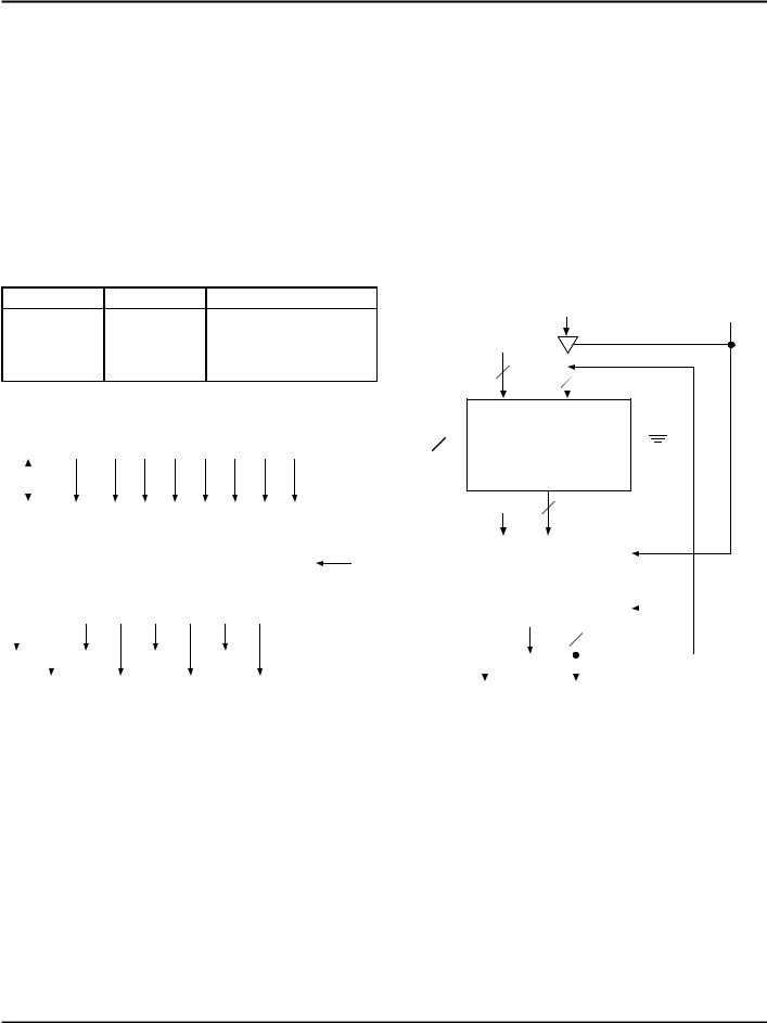
CHECK BITS
Figure 1. 32-Bit Configuration
Figure 2. 64-Bit Configuration
|
|
|
|
|
|
|
|
|
|
DATA |
|
|
|
|
|
|
CHECK BITS |
|
|
|
|
|
|
|
|
|
|||||||||||
|
|
|
|
|
BYTE3 |
|
BYTE2 |
|
BYTE1 |
BYTE0 |
C0 |
C1 |
C2 |
|
C3 |
|
C4 |
|
C5 |
|
C6 |
|
|
|
|
||||||||||||
|
|
|
|
|
|
|
|
|
|
|
|
|
|
|
|
|
|
|
|
|
|
|
|
|
|
|
|
|
|
|
|
|
|
|
|
||
|
|
|
31 |
24 23 |
16 15 |
8 7 |
0 |
|
|
|
|
|
|
|
|
|
|
|
|
|
|
|
|
|
|
|
|
||||||||||
|
|
|
|
|
|
|
|
|
|
|
|
|
|
Figure 3. 32-Bit Data Format |
|
|
|
|
|
|
|
|
2584 drw 07 |
||||||||||||||
|
|
|
|
|
|
|
|
|
|
|
|
|
|
|
|
|
|
|
|
|
|
|
|
|
|
|
|
|
|
||||||||
|
|
|
|
|
|
|
|
|
|
DATA |
|
|
|
|
|
|
|
|
|
|
|
|
|
|
|
|
CHECK BITS |
||||||||||
BYTE7 |
BYTE6 |
BYTE5 |
|
BYTE4 |
BYTE3 |
BYTE2 |
BYTE1 |
BYTE0 |
|
C0 |
|
C1 |
C2 |
|
C3 |
|
C4 |
C5 |
C6 |
C7 |
|||||||||||||||||
|
|
|
|
|
|
|
|
|
|
|
|
|
|
|
|
|
|
|
|
|
|
|
|
|
|
|
|
|
|
|
|
|
|||||
63 |
56 55 |
48 47 |
40 39 |
32 31 |
24 23 |
16 15 |
8 7 |
0 |
|
|
|
|
|
|
|
|
|
|
|
|
|
|
|
|
|
||||||||||||
2584 drw 08
Figure 4. 64-Bit Data Format
11.6 |
8 |

IDT49C460/A/B/C/D/E |
|
32-BIT CMOS ERROR DETECTION AND CORRECTION UNIT |
MILITARY AND COMMERCIAL TEMPERATURE RANGES |
32-BIT DATA WORD CONFIGURATION
A single IDT49C460 EDC unit, connected as shown in Figure 1, provides all the logic needed for single bit error correction and double bit error detection of a 32-bit data field. The identification code indicates 7 check bits are required. The CB7 pin should be HIGH.
Figure 3 indicates the 39-bit data format for two bytes of data and 7 check bits. Table 3 describes the operating mode available.
Table 6 indicates the data bits participating in the check bit generation. For example, check bit C0 is the exclusive-OR function of the 16 data input bits marked with an X. Check bits are generated and output in the Generate and Initialization Mode. Check bits from the respective latch are passed, unchanged, in the PASSTHRU or Diagnostic Generate Mode.
Syndrome bits are generated by an exclusive-OR or the
generated check bits with the read check bits. For example, Sn is the XOR of check bits Cn from those read with those generated. Table 7 indicates the decoding of the seven syndrome bits to identify the bit-in-error for a single bit error, or whether a double or triple bit error was detected. The all zero case indicates no errors detected.
In the Correct Mode, the syndrome bits are used to complement (correct) single bit errors in the data bits. For double or multiple error detection, the data available as input to the Data Out Latch is not defined.
Table 5 defines the bit definition for the Diagnostic Latch. As defined in Table 3, several modes will use the diagnostic check bits to determine syndrome bits or to pass as check bits to the SC0–7 outputs. The Internal Mode substitutes the indicated bit position for the external control signals.
|
|
BIT 0 |
|
|
|
CB0 DIAGNOSTIC |
|
|
|
|
|
|
|
|
|||
|
|
BIT 1 |
|
|
|
CB1 DIAGNOSTIC |
|
|
|
|
|
|
|
|
|||
|
|
BIT 2 |
|
|
|
CB2 DIAGNOSTIC |
|
|
|
|
|
|
|
|
|||
|
|
BIT 3 |
|
|
|
CB3 DIAGNOSTIC |
|
|
|
|
|
|
|
|
|||
|
|
BIT 4 |
|
|
|
CB4 DIAGNOSTIC |
|
|
|
|
|
|
|
|
|||
|
|
BIT 5 |
|
|
|
CB5 DIAGNOSTIC |
|
|
|
|
|
|
|
|
|||
|
|
BIT 6 |
|
|
|
CB6 DIAGNOSTIC |
|
|
|
|
|
|
|
|
|||
|
|
BIT 7 |
|
|
|
CB7 DIAGNOSTIC |
|
|
|
|
|
|
|
|
|||
|
|
BIT 8 |
|
|
|
CODE ID0 |
|
|
|
|
|
|
|
|
|
||
|
|
BIT 9 |
|
|
|
CODE ID1 |
|
|
|
|
|
|
|
|
|
||
|
|
BIT 10 |
|
|
|
DIAG MODE0 |
|
|
|
|
|
|
|
|
|
||
|
|
BIT 11 |
|
|
|
DIAG MODE1 |
|
|
|
|
|
|
|
|
|
||
|
|
BIT 12 |
|
|
|
CORRECT |
|
|
|
|
|
|
|
|
|
||
|
|
BIT 13–31 |
|
|
DON'T CARE |
|
|
|
|
|
|
|
|
|
|||
|
|
Table 5. 32-Bit Diagnostic Latch Coding Format |
2584 drw 05 |
|
|
|
|
|
|
||||||||
|
|
|
|
|
|
|
|
|
|||||||||
Generated |
|
|
|
|
|
|
|
Participating Data Bits |
|
|
|
|
|
|
|||
Check Bits |
Parity |
0 |
1 |
2 |
3 |
4 |
5 |
6 |
7 |
8 |
9 |
10 |
11 |
12 |
13 |
14 |
15 |
C0 |
Even (XOR) |
X |
|
|
|
X |
|
X |
X |
X |
X |
|
X |
|
|
X |
|
C1 |
Even (XOR) |
X |
X |
X |
|
X |
|
X |
|
X |
|
X |
|
X |
|
|
|
C2 |
Odd (XNOR) |
X |
|
|
X |
X |
|
|
X |
|
X |
X |
|
|
X |
|
X |
C3 |
Odd (XNOR) |
X |
X |
|
|
|
X |
X |
X |
|
|
|
X |
X |
X |
|
|
C4 |
Even (XOR) |
|
|
X |
X |
X |
X |
X |
X |
|
|
|
|
|
|
X |
X |
C5 |
Even (XOR) |
|
|
|
|
|
|
|
|
X |
X |
X |
X |
X |
X |
X |
X |
C6 |
Even (XOR) |
X |
X |
X |
X |
X |
X |
X |
X |
|
|
|
|
|
|
|
|
|
|
|
|
|
|
|
|
|
|
|
|
|
|
|
|
|
2584 tbl 06 |
Generated |
|
|
|
|
|
|
|
Participating Data Bits |
|
|
|
|
|
|
|||
Check Bits |
Parity |
16 |
17 |
18 |
19 |
20 |
21 |
22 |
23 |
24 |
25 |
26 |
27 |
28 |
29 |
30 |
31 |
C0 |
Even (XOR) |
|
X |
X |
X |
|
X |
|
|
|
|
X |
|
X |
X |
|
X |
C1 |
Even (XOR) |
X |
X |
X |
|
X |
|
X |
|
X |
|
X |
|
X |
|
|
|
C2 |
Odd (XNOR) |
X |
|
|
X |
X |
|
|
X |
|
X |
X |
|
|
X |
|
X |
C3 |
Odd (XNOR) |
X |
X |
|
|
|
X |
X |
X |
|
|
|
X |
X |
X |
|
|
C4 |
Even (XOR) |
|
|
X |
X |
X |
X |
X |
X |
|
|
|
|
|
|
X |
X |
C5 |
Even (XOR) |
|
|
|
|
|
|
|
|
X |
X |
X |
X |
X |
X |
X |
X |
C6 |
Even (XOR) |
|
|
|
|
|
|
|
|
X |
X |
X |
X |
X |
X |
X |
X |
|
|
|
|
|
|
|
|
|
|
|
|
|
|
|
|
|
2584 tbl 07 |
|
|
Table 6. 32–Bit Modified Hamming Code–Check Bit Encode Chart |
|
|
|
|
|
|
|||||||||
|
|
|
|
|
|
|
|
|
|
|
|
|
|
|
|
|
|
11.6 |
9 |

IDT49C460/A/B/C/D/E |
|
32-BIT CMOS ERROR DETECTION AND CORRECTION UNIT |
MILITARY AND COMMERCIAL TEMPERATURE RANGES |
|
Hex |
0 |
1 |
2 |
3 |
4 |
5 |
6 |
7 |
Syndrome |
S6 |
0 |
0 |
0 |
0 |
1 |
1 |
1 |
1 |
Bits |
S5 |
0 |
0 |
1 |
1 |
0 |
0 |
1 |
1 |
|
S4 |
0 |
1 |
0 |
1 |
0 |
1 |
0 |
1 |
Hex S3 |
S2 |
S1 |
S0 |
|
|
|
|
|
0 |
0 |
0 |
0 |
0 |
* C4 C5 T C6 T T 30 |
|||
1 |
0 |
0 |
0 |
1 |
C0 T T 14 T M M T |
|||
2 |
0 |
0 |
1 |
0 |
C1 T |
T M T 2 24 T |
||
3 |
0 |
0 |
1 |
1 |
T 18 |
8 T M |
T T M |
|
4 |
0 |
1 |
0 |
0 |
C2 T |
T 15 T |
3 25 T |
|
5 |
0 |
1 |
0 |
1 |
T 19 9 T M T T 31 |
|||
6 |
0 |
1 |
1 |
0 |
T 20 10 T M T T M |
|||
7 |
0 |
1 |
1 |
1 |
M T T M T 4 |
26 T |
||
8 |
1 |
0 |
0 |
0 |
C3 T T M T 5 |
27 T |
||
9 |
1 |
0 |
0 |
1 |
T 21 11 T M |
T T M |
||
A 1 0 1 0 |
T 22 12 T 1 T T M |
|||||||
B 1 0 1 1 |
17 T T M T 6 |
28 T |
||||||
C 1 1 0 0 |
T 23 13 T M T T M |
|||||||
D 1 1 0 1 |
M T T M T 7 |
29 T |
||||||
E 1 1 1 0 |
16 T T M T M M T |
|||||||
F 1 1 1 1 |
T M M T 0 T T M |
|||||||
NOTES: |
|
|
|
|
|
|
2584 tbl 08 |
|
1.* = No errors detected
2.Number = The number of the single bit-in-error
3.T = Two errors detected
4.M = Three or more errors detected
Table 7. Syndrome Decode to Bit-in-Error (32-Bit)
64-BIT DATA WORD CONFIGURATION
Two IDT49C460 EDC units, connected as shown in Figure 2, provide all the logic needed for single bit error detection and double bit error detection of a 64-bit data field. Table 4 gives the CODE ID1,0 values needed for distinguishing the upper 32 bits from the lower 32 bits. Valid syndrome, check bits and the ERROR and MULT ERROR signals come from the IC with the CODE ID1,0 = 11. Control signals not indicated are connected to both units in parallel. The EDC with the CODE ID1,0 = 10 has the OESC grounded. The OESC selects the syndrome bits from the EDC with CODE ID1,0 = 11 and also controls the check bit buffers from memory.
Data In bits 0 through 31 are connected to the same numbered inputs of the EDC unit with CODE ID1,0 = 10, while Data In bits 32 through 63 are connected to Data Inputs 0 to 31, respectively, for the EDC unit with CODE ID1,0 = 11.
Figure 4 indicates the 72-bit data format of 8 bytes of data and 8 check bits. Check bits are input to the EDC unit with CODE ID1,0 = 10 through a three-state buffer unit such as the IDT74FCT244. Correction of single bit errors of the 64-bit configuration requires a feedback of syndrome bits from the upper EDC unit to the lower EDC unit. The MUX shown on the functional block diagram is used to select the CB0–7 pins as the syndrome bits rather than internally generated syndrome bits.
Table 3 describes the operating modes available for the 64/ 72 configuration.
Table 11 indicates the data bits participating in the check bit generation. For example, check bit C0 is the exclusive-OR function of the 32 data input bits marked with an X. Check bits are generated and output in the Generate and Initialization modes. Check bits are passed as stored in the PASSTHRU or Diagnostic Generate modes.
Syndrome bits are generated by an exclusive-OR of the generated check bits with the read check bits. For example, Sn is the XOR of check bits Cn from those read with those generated. Table 9 indicates the decoding of the 8 syndrome bits to determine the bit in error for a single bit error or whether a double or triple bit error was detected. The all zero case indicates no errors detected.
In the Correct Mode, the syndrome bits are used to complement (correct) single bit errors in the data bits. For double or multiple error detection, the data available as input to the Data Out Latch is not defined.
Tables 8A and 8B define the bit definition for the Diagnostic Latch. As defined in Table 3, several modes will use the Diagnostic Check Bits to determine syndrome bits or to pass as check bits to the SC0–7 outputs. The Internal Mode substitutes the indicated bit position for the external control signals.
Performance data is provided in Table 10, relating a single IDT49C460 EDC with the two cascaded units of Figure 2. As indicated, a summation of propagation delays is required from the cascading arrangement of EDC units.
Bit |
Internal Function |
||
0 |
CB0 DIAGNOSTIC |
||
1 |
CB1 DIAGNOSTIC |
||
2 |
CB2 DIAGNOSTIC |
||
3 |
CB3 DIAGNOSTIC |
||
4 |
CB4 DIAGNOSTIC |
||
5 |
CB5 DIAGNOSTIC |
||
6 |
CB6 DIAGNOSTIC |
||
7 |
CB7 DIAGNOSTIC |
||
8 |
CODE ID0 |
LOWER 32-BIT |
|
9 |
CODE ID1 |
LOWER 32-BIT |
|
10 |
DIAG MODE0 |
LOWER 32-BIT |
|
11 |
DIAG MODE1 |
LOWER 32-BIT |
|
12 |
CORRECT LOWER 32-BIT |
||
13–31 |
DON'T CARE |
|
|
32–39 |
DON'T CARE |
|
|
40 |
CODE ID0 |
UPPER 32-BIT |
|
41 |
CODE ID1 |
UPPER 32-BIT |
|
42 |
DIAG MODE0 |
UPPER 32-BIT |
|
43 |
DIAG MODE1 |
UPPER 32-BIT |
|
44 |
CORRECT UPPER 32-BIT |
||
45–63 |
DON'T CARE |
|
|
2584 tbl 09
Table 8A. 64-Bit Diagnostic Latch–Coding Format
(Diagnostic and Correct Mode)
11.6 |
10 |
 Loading...