


IDT IDT54FCT821A, IDT54FCT821B, IDT54FCT821C, IDT54FCT823A, IDT54FCT823B User Manual
...IDT54FCT821ADB
®
Integrated Device Technology, Inc.
HIGH-PERFORMANCE |
IDT54/74FCT821A/B/C |
|
CMOS BUS INTERFACE |
IDT54/74FCT823A/B/C |
|
REGISTERS |
IDT54/74FCT824A/B/C |
|
IDT54/74FCT825A/B/C |
||
|
||
|
|
FEATURES:
•Equivalent to AMD’s Am29821-25 bipolar registers in pinout/function, speed and output drive over full temperature and voltage supply extremes
•IDT54/74FCT821A/823A/824A/825A equivalent to FAST™ speed
•IDT54/74FCT821B/823B/824B/825B 25% faster than FAST
•IDT54/74FCT821C/823C/824C/825C 40% faster than FAST
•Buffered common Clock Enable (EN) and asynchronous Clear input (CLR)
•IOL = 48mA (commercial) and 32mA (military)
•Clamp diodes on all inputs for ringing suppression
•CMOS power levels (1mW typ. static)
•TTL input and output compatibility
•CMOS output level compatible
•Substantially lower input current levels than AMD’s bipolar Am29800 series (5μA max.)
•Product available in Radiation Tolerant and Radiation Enhanced versions
•Military product compliant to MIL-STD-883, Class B
DESCRIPTION:
The IDT54/74FCT800 series is built using an advanced dual metal CMOS technology.
The IDT54/74FCT820 series bus interface registers are designed to eliminate the extra packages required to buffer existing registers and provide extra data width for wider address/data paths or buses carrying parity. The IDT54/ 74FCT821 are buffered, 10-bit wide versions of the popular ‘374 function. The IDT54/74FCT823 and IDT54/74FCT824 are 9-bit wide buffered registers with Clock Enable (EN) and Clear (CLR) – ideal for parity bus interfacing in high-perform- ance microprogrammed systems. The IDT54/74FCT825 are 8-bit buffered registers with all the ‘823 controls plus multiple enables (OE1, OE2, OE3) to allow multiuser control of the interface, e.g., CS, DMA and RD/WR. They are ideal for use as an output port requiring HIGH IOL/IOH.
All of the IDT54/74FCT800 high-performance interface family are designed for high-capacitance load drive capability, while providing low-capacitance bus loading at both inputs and outputs. All inputs have clamp diodes and all outputs are designed for low-capacitance bus loading in high-impedance state.
FUNCTIONAL BLOCK DIAGRAMS
IDT54/74FCT821/823/825
D0 |
DN |
EN |
|
CLR |
|
D CL Q |
D CL Q |
CP Q |
CP Q |
CP |
|
OE |
|
Y0 |
YN |
The IDT logo is a registered trademark of Integrated Device Technology, Inc. |
2608 cnv* 01 |
|
|
FAST is a trademark of National Semiconductor Co. |
|
IDT54/74FCT824
D0 |
DN |
EN
CLR |
|
D CL Q |
D CL Q |
CP Q |
CP Q |
CP |
|
OE |
|
Y0 |
YN |
2608 cnv* 02
MILITARY AND COMMERCIAL TEMPERATURE RANGES |
MAY 1992 |
|
©1992 Integrated Device Technology, Inc. |
7.19 |
DSC-4618/2 |
1

IDT54/74FCT821/823/824/825A/B/C |
|
HIGH-PERFORMANCE CMOS BUS INTERFACE REGISTERS |
MILITARY AND COMMERCIAL TEMPERATURE RANGES |
PIN CONFIGURATIONS
IDT54/74FCT821 10-BIT REGISTER
OE |
|
|
|
1 |
|
24 |
|
|
|
VCC |
INDEX |
D1 |
D0 |
OE NC VCC Y0 Y1 |
|
|||||||
|
|
|
|
|
|
|
|
|||||||||||||||
D0 |
|
|
|
2 |
|
23 |
|
|
|
Y0 |
|
|
||||||||||
|
|
|
|
|
|
|
|
|
||||||||||||||
|
|
|
|
|
|
|
|
|
|
|
|
|
|
|
||||||||
D1 |
|
|
|
3 |
|
22 |
|
|
|
Y1 |
|
4 |
3 |
2 |
1 28 27 26 |
|
||||||
|
|
|
|
|
|
|
|
|
||||||||||||||
D2 |
|
|
|
4 |
P24-1 |
21 |
|
|
|
Y2 |
D2 |
Y2 |
||||||||||
|
|
|
|
|
|
|||||||||||||||||
D3 |
|
|
|
5 |
D24-1 |
20 |
|
|
|
Y3 |
5 |
|
|
|
|
25 |
||||||
|
|
|
|
|
|
|
|
|
|
|||||||||||||
|
|
|
|
|
|
D3 |
6 |
|
|
|
|
24 |
Y3 |
|||||||||
D4 |
|
|
|
6 |
E24-1 |
19 |
|
|
|
Y4 |
|
|
|
|
||||||||
|
|
|
|
|
|
D4 |
7 |
|
|
|
|
23 |
Y4 |
|||||||||
D5 |
|
|
|
7 |
& |
18 |
|
|
|
Y5 |
|
|
|
|
||||||||
|
|
|
|
|
|
NC |
8 |
|
L28-1 |
22 |
NC |
|||||||||||
D6 |
|
|
|
8 |
SO24-2 |
17 |
|
|
|
Y6 |
|
|||||||||||
|
|
|
|
|
|
D5 |
9 |
|
|
|
|
21 |
Y5 |
|||||||||
D7 |
|
|
|
9 |
|
16 |
|
|
|
Y7 |
|
|
|
|
||||||||
|
|
|
|
|
|
|
D6 |
10 |
|
|
|
|
20 |
Y6 |
||||||||
|
|
|
|
|
|
|
|
|
|
|
||||||||||||
D8 |
|
|
|
10 |
|
15 |
|
|
|
Y8 |
D7 |
11 |
|
|
|
|
19 |
Y7 |
||||
|
|
|
|
|
|
|
|
|
|
|
||||||||||||
D9 |
|
|
|
11 |
|
14 |
|
|
|
Y9 |
|
1213 14 15 16 17 18 |
|
|||||||||
|
|
|
|
|
|
|
|
|
||||||||||||||
GND |
|
|
|
12 |
|
13 |
|
|
|
CP |
|
D8 |
D9 |
GND NC CP Y9 |
Y8 |
|
||||||
|
|
|
|
|
|
|
|
|
||||||||||||||
|
|
|
|
|
|
|
|
|
|
|
|
|
|
|
|
|
||||||
DIP/SOIC/CERPACK |
|
|
|
|
LCC |
|
|
|||||||||||||||
|
|
|
|
|
|
TOP VIEW |
|
|
|
|
|
TOP VIEW |
|
|
||||||||
IDT54/74FCT823/824 9-BIT REGISTERS |
|
|
|
|
|
|
|
|||||||||||||||
OE |
|
1 |
|
24 |
|
|
|
|
VCC |
INDEX |
D1 |
D0 OE NC VCC Y0 Y1 |
|
|||||||||
|
|
|
|
|
|
|
||||||||||||||||
D0 |
|
|
|
2 |
|
23 |
|
|
|
|
Y0 |
|
|
|||||||||
|
|
|
|
|
|
|
|
|
|
|||||||||||||
|
|
|
|
|
|
|
|
|
|
|
|
|
|
|||||||||
D1 |
|
3 |
|
22 |
|
|
|
|
Y1 |
|
4 |
3 |
2 |
1 28 27 26 |
|
|||||||
|
|
|
|
|
|
|
|
|||||||||||||||
D2 |
|
4 |
P24-1 |
21 |
|
|
|
|
Y2 |
D2 |
|
|||||||||||
|
|
|
|
|
|
|||||||||||||||||
D3 |
|
|
|
5 |
D24-1 |
20 |
|
|
|
|
Y3 |
5 |
|
|
|
|
25 |
Y2 |
||||
|
|
|
|
|
|
|
|
|
|
|
||||||||||||
|
|
|
|
|
D3 |
6 |
|
|
|
|
24 |
Y3 |
||||||||||
D4 |
|
|
|
6 SO24-2 |
19 |
|
|
|
|
Y4 |
|
|
|
|
||||||||
|
|
|
|
|
|
|
D4 |
7 |
|
|
|
|
23 |
Y4 |
||||||||
D5 |
|
|
|
7 |
& |
18 |
|
|
|
|
Y5 |
|
|
|
|
|||||||
|
|
|
|
|
NC |
8 |
|
|
L28-1 |
22 |
NC |
|||||||||||
D6 |
|
|
|
8 |
E24-1 |
17 |
|
|
|
|
Y6 |
|
|
|||||||||
|
|
|
|
|
D5 |
9 |
|
|
|
|
21 |
Y5 |
||||||||||
D7 |
|
|
|
9 |
|
16 |
|
|
|
Y7 |
|
|
|
|
||||||||
|
|
|
D6 |
10 |
|
|
|
|
20 |
Y6 |
||||||||||||
|
|
|
|
|
|
|
||||||||||||||||
D8 |
|
10 |
15 |
|
|
|
|
Y8 |
D7 |
11 |
|
|
|
|
19 |
Y7 |
||||||
|
|
|
|
|
|
|
|
|
||||||||||||||
CLR |
|
11 |
14 |
|
|
|
|
EN |
|
1213 14 15 16 17 18 |
|
|||||||||||
|
|
|
|
|
|
|
||||||||||||||||
GND |
|
12 |
13 |
|
|
|
|
CP |
|
D8 |
CLR |
GND |
NC CP EN Y8 |
|
||||||||
|
|
|
|
|
|
|
||||||||||||||||
|
|
|
|
|
|
|
|
|
|
|
|
|
|
|
|
|
||||||
|
DIP/SOIC/CERPACK |
|
|
|
|
LCC |
|
|
||||||||||||||
|
|
|
|
|
|
TOP VIEW |
|
|
|
|
|
TOP VIEW |
|
|||||||||
IDT54/74FCT825 8-BIT REGISTER |
|
|
|
|
|
|
|
|
||||||||||||||
OE1 |
|
|
|
1 |
|
24 |
|
|
|
VCC |
INDEX |
D0 |
OE2 |
OE1 |
NC VCC |
OE3 Y0 |
|
|||||
|
|
|
|
|
|
|
||||||||||||||||
OE2 |
|
|
|
|
2 |
|
23 |
|
|
|
OE3 |
|
|
|||||||||
|
|
|
|
|
|
|
|
|
|
|||||||||||||
|
|
|
|
|
|
|
|
|
|
|
|
|
|
|
||||||||
D0 |
|
|
|
3 |
|
22 |
|
|
|
Y0 |
|
4 |
3 |
2 |
1 28 27 26 |
|
||||||
|
|
|
|
|
|
|
|
|||||||||||||||
D1 |
|
|
|
4 |
P24-1 |
21 |
|
|
|
Y1 |
D1 |
Y1 |
||||||||||
|
|
|
|
|
||||||||||||||||||
D2 |
|
|
|
|
5 |
D24-1 |
20 |
|
|
|
Y2 |
5 |
|
|
|
|
25 |
|||||
|
|
|
|
|
|
|
|
|
|
|
||||||||||||
|
|
|
|
|
|
D2 |
6 |
|
|
|
|
24 |
Y2 |
|||||||||
D3 |
|
|
|
|
6 |
E24-1 |
19 |
|
|
|
Y3 |
|
|
|
|
|||||||
|
|
|
|
|
|
D3 |
7 |
|
|
|
|
23 |
Y3 |
|||||||||
D4 |
|
|
|
|
7 |
& |
18 |
|
|
|
Y4 |
|
|
|
|
|||||||
|
|
|
|
|
|
NC |
8 |
|
|
L28-1 |
22 |
NC |
||||||||||
D5 |
|
|
|
|
8 |
SO24-2 17 |
|
|
|
Y5 |
|
|
||||||||||
|
|
|
|
|
|
D4 |
9 |
|
|
|
|
21 |
Y4 |
|||||||||
D6 |
|
|
|
|
9 |
|
16 |
|
|
|
Y6 |
|
|
|
|
|||||||
|
|
|
|
|
|
D5 |
10 |
|
|
|
|
20 |
Y5 |
|||||||||
D7 |
|
|
|
|
|
|
|
|
|
|||||||||||||
|
|
|
10 |
15 |
|
|
|
Y7 |
D6 |
11 |
|
|
|
|
19 |
Y6 |
||||||
|
|
|
|
|
|
|
|
|
||||||||||||||
CLR |
|
|
|
11 |
14 |
|
|
|
EN |
|
1213 14 1516 17 18 |
|
||||||||||
|
|
|
|
|
|
|
||||||||||||||||
GND |
|
|
|
12 |
13 |
|
|
|
CP |
|
D7 |
CLR GND |
NC CP |
EN Y7 |
|
|||||||
|
|
|
|
|
|
|
||||||||||||||||
|
|
|
|
|
|
|
|
|
|
|
|
|
|
|
|
|
||||||
|
|
DIP/SOIC/CERPACK |
|
|
|
|
|
LCC |
|
|
||||||||||||
|
|
|
|
|
|
|
TOP VIEW |
|
|
|
|
|
|
TOP VIEW |
|
|||||||
LOGIC SYMBOLS
|
10 |
10 |
D |
D |
|
|
Q |
Y |
|
CP |
|
CP |
|
|
OE |
|
|
2608 cnv* 03
D |
9 |
9 |
D |
||
|
Q |
Y |
|
CP EN CLR |
|
CP
EN
CLR
OE
2608 cnv* 04
|
8 |
|
8 |
|
D |
D |
|||
|
||||
|
|
Q |
Y |
|
|
|
CP EN CLR |
|
|
|
|
|
|
CP
EN 
CLR
OE1 
OE2 
OE3 
2608 cnv* 05
7.19 |
2 |
IDT54/74FCT821/823/824/825A/B/C |
|
HIGH-PERFORMANCE CMOS BUS INTERFACE REGISTERS |
MILITARY AND COMMERCIAL TEMPERATURE RANGES |
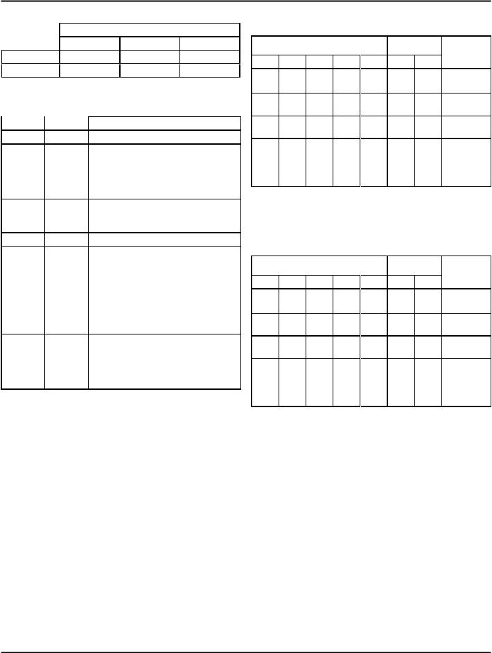
PRODUCT SELECTOR GUIDE
|
|
Device |
|
|
10-Bit |
9-Bit |
8-Bit |
Non-inverting |
54/74FCT821A/B/C |
54/74FCT823A/B/C |
54/74FCT825A/B/C |
Inverting |
|
54/74FCT824A/B/C |
|
|
|
|
2608 tbl 01 |
PIN DESCRIPTION
Name |
I/O |
Description |
DI |
I |
The D flip-flop data inputs. |
CLR |
I |
For both inverting and non-inverting |
|
|
registers, when the clear input is LOW |
|
|
and OE is LOW, the QI outputs are |
|
|
LOW. When the clear input is HIGH, |
|
|
data can be entered into the register. |
CP |
I |
Clock Pulse for the Register; enters |
|
|
data into the register on the LOW-to- |
|
|
HIGH transition. |
YI , YI |
O |
The register three-state outputs. |
EN |
I |
Clock Enable. When the clock enable |
|
|
is LOW, data on the D I input is |
|
|
transferred to the QI output on the |
|
|
LOW-to-HIGH clock transition. When |
|
|
the clock enable is HIGH, the QI |
|
|
outputs do not change state, |
|
|
regardless of the data or clock input |
|
|
transitions. |
OE |
I |
Output Control. When the OE input is |
|
|
HIGH, the Y I outputs are in the high |
|
|
impedance state. When the OE input is |
|
|
LOW, the TRUE register data is |
|
|
present at the Y I outputs. |
|
|
2608 tbl 10 |
FUNCTION TABLE(1)
IDT54/74FCT821/823/825
|
|
Inputs |
|
|
Internal/ |
|
|
|
|
|
|
Outputs |
|
||
|
|
|
|
|
|
||
OE |
CLR |
EN |
DI |
CP |
QI |
YI |
Function |
H |
H |
L |
L |
− |
L |
Z |
High Z |
H |
H |
L |
H |
− |
H |
Z |
|
H |
L |
X |
X |
X |
L |
Z |
Clear |
L |
L |
X |
X |
X |
L |
L |
|
H |
H |
H |
X |
X |
NC |
Z |
Hold |
L |
H |
H |
X |
X |
NC |
NC |
|
H |
H |
L |
L |
− |
L |
Z |
Load |
H |
H |
L |
H |
− |
H |
Z |
|
L |
H |
L |
L |
− |
L |
L |
|
L |
H |
L |
H |
− |
H |
H |
|
NOTE: |
|
|
|
|
|
|
2608 tbl 02 |
1.H = HIGH, L = LOW, X = Don’t Care, NC = No Change, − = LOW-to-HIGH Transition, Z = High Impedance
FUNCTION TABLE(1)
IDT54/74FCT824
|
|
Inputs |
|
|
Internal/ |
|
|
|
|
|
|
Outputs |
|
||
|
|
|
|
|
|
||
OE |
CLR |
EN |
DI |
CP |
QI |
YI |
Function |
H |
H |
L |
L |
− |
H |
Z |
High Z |
H |
H |
L |
H |
− |
L |
Z |
|
H |
L |
X |
X |
X |
L |
Z |
Clear |
L |
L |
X |
X |
X |
L |
L |
|
H |
H |
H |
X |
X |
NC |
Z |
Hold |
L |
H |
H |
X |
X |
NC |
NC |
|
H |
H |
L |
L |
− |
H |
Z |
Load |
H |
H |
L |
H |
− |
L |
Z |
|
L |
H |
L |
L |
− |
H |
H |
|
L |
H |
L |
H |
− |
L |
L |
|
NOTE: |
|
|
|
|
|
|
2608 tbl 03 |
1.H = HIGH, L = LOW, X = Don’t Care, NC = No Change, − = LOW-to- HIGH Transition, Z = High Impedance
7.19 |
3 |
 Loading...