


IDT54FCT861A
IDT IDT54FCT861A, IDT54FCT861B, IDT54FCT863A, IDT54FCT863B, IDT74FCT861A User Manual
...
Integrated Device Technology, Inc.
MILITARY AND COMMERCIAL TEMPERATURE RANGES APRIL 1994
1994 Integrated Device Technology, Inc. 7.23 DSC-4620/3
HIGH-PERFORMANCE
CMOS BUS
TRANSCEIVERS
The IDT logo is a registered trademark of Integrated Device Technology, Inc.
FAST is a trademark of National Semiconductor Co.
FEATURES:
• Equivalent to AMD’s Am29861-64 bipolar registers in
pinout/function, speed and output drive over full tempera-
ture and voltage supply extremes
• IDT54/74FCT861A/863A equivalent to FAST speed
• IDT54/74FCT861B/863B 25% faster than FAST
• High-speed symmetrical bidirectional transceivers
•IOL = 48mA (commercial) and 32mA (military)
• Clamp diodes on all inputs for ringing suppression
• CMOS power levels (1mW typ. static)
• TTL input and output level compatible
• CMOS output level compatible
• Substantially lower input current levels than AMD’s
bipolar Am29800 Series (5µA max.)
• Product available in Radiation Tolerant and Radiation
Enhanced versions
• Military product compliant to MIL-STD-883, Class B
DESCRIPTION:
The IDT54/74FCT800 series is built using an advanced
dual metal CMOS technology.
The IDT54/74FCT860 series bus transceivers provide
high-performance bus interface buffering for wide
data/address paths or buses carrying parity. The
IDT54/74FCT863 9-bit transceivers have NAND-ed output
enables for maximum control flexibility.
All of the IDT54/74FCT800 high-performance interface
family are designed for high-capacitance load drive capability
while providing low-capacitance bus loading at both inputs
and outputs. All inputs have clamp diodes and all outputs are
designed for low-capacitance bus loading in the high- im-
pedance state.
FUNCTIONAL BLOCK DIAGRAMS
IDT54/74FCT861 IDT54/74FCT863
T
0
T
1
OERT
9
-
R
0
R
1
OETR
9
-
IDT54/74FCT861A/B
IDT54/74FCT863A/B
1
2610 drw 01
T
0
T
1
OERT
8
-
R
0
R
1
OETR
8
- OET
12
OER
12
PRODUCT SELECTOR GUIDE
Device
10-Bit 9-Bit
Non-inverting IDT54/74FCT861 IDT54/74FCT863
查询IDT54FCT683AD供应商

IDT54/74FCT861A/B, IDT54/74FCT863A/B
HIGH-PERFORMANCE CMOS BUS TRANSCEIVERS MILITARY AND COMMERCIAL TEMPERATURE RANGES
7.23 2
PIN CONFIGURATIONS
IDT54/74FCT861 10-BIT TRANSCEIVERS
5
6
7
8
9
10
11
12
GND
OER
R
0
R
1
1
2
3
4
24
23
22
21
20
19
18
17
Vcc
16
15
14
13
P24-1,
D24-1,
E24-1
&
SO24-2
T
0
R
2
R
3
R
4
R
5
R
6
T
1
T
2
T
3
T
4
T
5
T
6
T
7
R
7
R
8
T
8
1
OER
2
OET
2
OET
1
DIP/CERPACK/SOIC
TOP VIEW
2610 drw 02
5
6
7
8
9
10
11
L28-1
25
24
23
22
21
20
19
INDEX
R2
R3
R4
R
5
R6
R7
NC
Vcc
T
0
T
1
NC
NC
NC
T
2
T3
T4
T5
T6
T7
R
0
R
1
GND
R
8
T
8
OER
OER
2
OET
1
OET
2
12 13 14 15 16 17 18
432
1
28 27 26
LOGIC SYMBOLS
LCC
TOP VIEW
5
6
7
8
9
10
11
12
GND
OER
R
0
R
1
1
2
3
4
24
23
22
21
20
19
18
17
Vcc
16
15
14
13
P24-1,
D24-1,
E24-1
&
SO24-2
T
0
R
2
R
3
R
4
R
5
R
6
T
1
T
2
T
3
T
4
T
5
T
6
T
7
R
7
R
8
R
9
T
8
T
9
OET
LCC
TOP VIEW
DIP/CERPACK/SOIC
TOP VIEW
5
6
7
8
9
10
11
L28-1
25
24
23
22
21
20
19
INDEX
R2
R3
R4
R
5
R6
R7
NC
Vcc
T
0
T1
NC
NC
NC
T
2
T3
T4
T5
T6
T7
R
0
R
1
GND
R
8
R9
T
8
T
9
OET
OER
12 13 14 15 16 17 18
432
1
28 27 26
IDT54/74FCT863 9-BIT TRANSCEIVERS
IDT54/74FCT863IDT54/74FCT861
TR
10 10
OET
OER
OET1
OET2
2610 drw 03
TR
99
OER1
OER2
IDT54/74FCT861A/B, IDT54/74FCT863A/B
HIGH-PERFORMANCE CMOS BUS TRANSCEIVERS MILITARY AND COMMERCIAL TEMPERATURE RANGES
7.23 3
PIN DESCRIPTION
Name I/O Description
IDT54/74FCT861
OER
I When LOW in conjunction with
OET
HIGH
activates the RECEIVE mode.
OET
I When LOW in conjunction with
OER
HIGH
activates the TRANSMIT mode.
R
I I/O 10-bit RECEIVE input/output.
T
I I/O 10-bit TRANSMIT input/output.
IDT54/74FCT863
OER
I I When LOW in conjunction with
OET
I HIGH
activates the RECEIVE mode.
OET
I I When LOW in conjunction with
OER
I HIGH
activates the TRANSMIT mode.
R
I I/O 9-bit RECEIVE input/output.
T
I I/O 9-bit TRANSMIT input/output.
2610 tbl 01
CAPACITANCE (TA = +25°C, f = 1.0MHz)
Symbol Parameter
(1)
Conditions Typ. Max. Unit
C
IN Input Capacitance V IN = 0V 6 10 pF
C
I/O I/O Capacitance VOUT = 0V 8 12 pF
NOTE: 2610 tbl 04
1. This parameter is guaranteed by characterization but not tested.
ABSOLUTE MAXIMUM RATINGS
(1)
Symbol Rating Commercial Military Unit
V
TERM
(2)
Terminal Voltage –0.5 to +7.0 –0.5 to +7.0 V
with Respect
to GND
V
TERM
(3)
Terminal Voltage –0.5 to VCC –0.5 to VCC V
with Respect
to GND
T
A Operating 0 to +70 –55 to +125 °C
Temperature
T
BIAS Temperature –55 to +125 –65 to +135 °C
Under Bias
T
STG Storage –55 to +125 –65 to +150 °C
Temperature
P
T Power Dissipation 0.5 0.5 W
I
OUT DC Output Current 120 120 mA
NOTES: 2610 tbl 03
1. Stresses greater than those listed under ABSOLUTE MAXIMUM
RATINGS may cause permanent damage to the device. This is a stress
rating only and functional operation of the device at these or any other
conditions above those indicated in the operational sections of this
specification is not implied. Exposure to absolute maximum rating
conditions for extended periods may affect reliability. No terminal voltage
may exceed V
CC by +0.5V unless otherwise noted.
2. Inputs and V
CC terminals only.
3. Outputs and I/O terminals only.
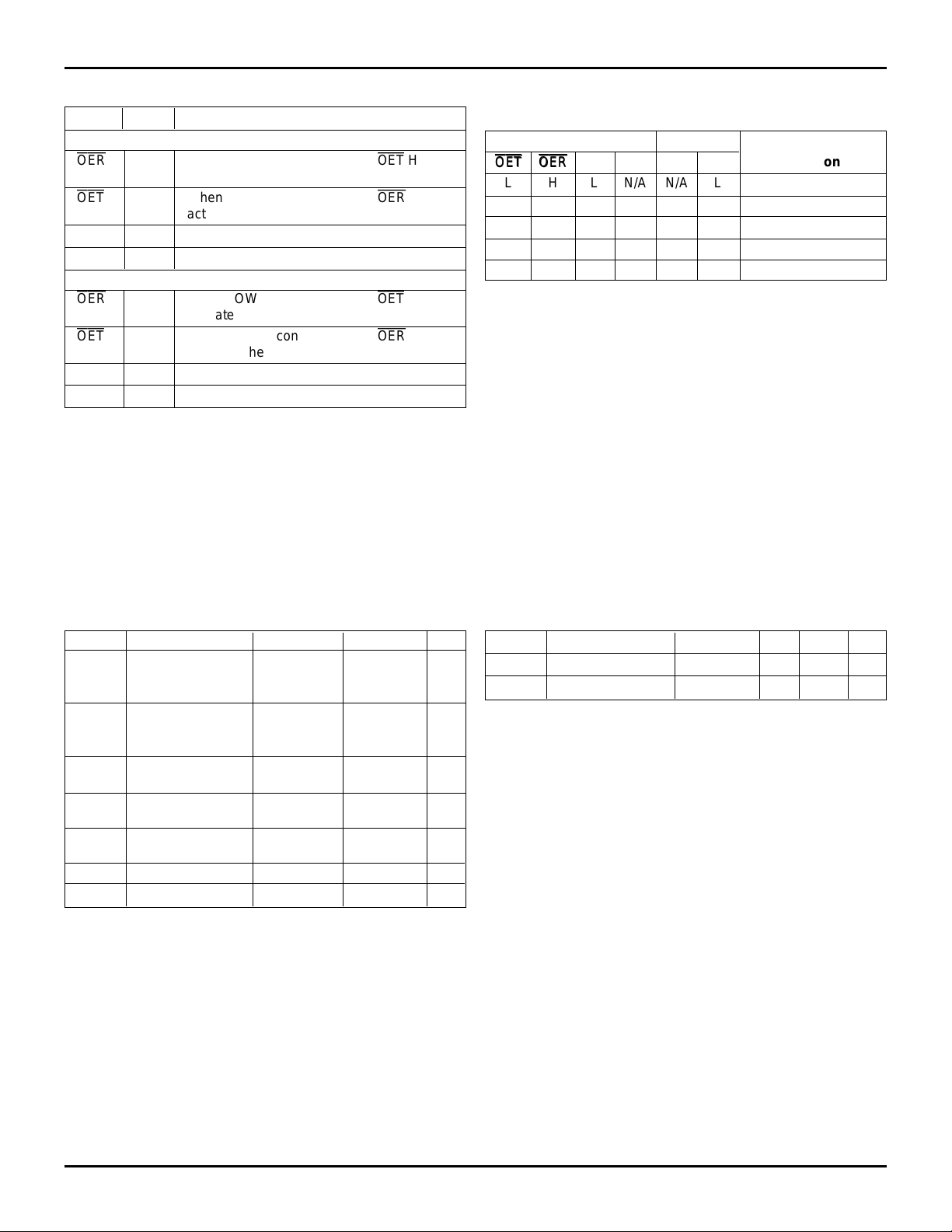
FUNCTION TABLE
(1)
IDT54/74FCT861/863 (Non-inverting)
Inputs Outputs
OET
OET
OER
OER
R
I T I RI TI Function
L H L N/A N/A L Transmitting
L H H N/A N/A H Transmitting
H L N/A L L N/A Receiving
H L N/A H H N/A Receiving
H H X X Z Z High Z
NOTE: 2610 tbl 02
1. H = HIGH, L = LOW, Z = High Impedance, X = Don’t Care, N/A = Not
Applicable.
 Loading...