


MC78L24A
Fairchild Semiconductor MC78L24A, MC78L18A, MC78L15A, MC78L12A, MC78L05AA Datasheet
...
©2002 Fairchild Semiconductor Corporation
www.fairchildsemi.com
Rev. 1.0.4
Features
• Maximum Output Current of 100mA
• Output Voltage of 5V, 8V, 12V, 15V, 18V and 24V
• Thermal Overload Protection
• Short Circuit Current Limiting
• Output Voltage Offered in ±5% Tolerance
Description
The MC78LXXA/LM78LXXA/MC78L05AA series of
fixed voltage monolithic integrated circuit voltage
regulators are suitable for application that required supply
current up to 100mA.
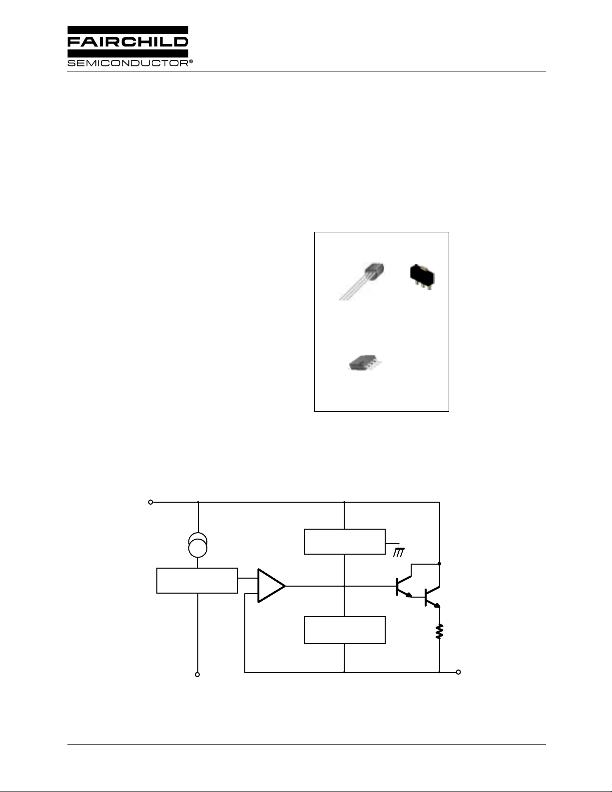
TO-92
1. Output 2. GND 3. Input
8-SOP
1. Output 2. GND 3. GND 4. NC
5. NC 6. GND 7. GND 8. Input
1
1
SOT-89
1
GND
2
3
23
8
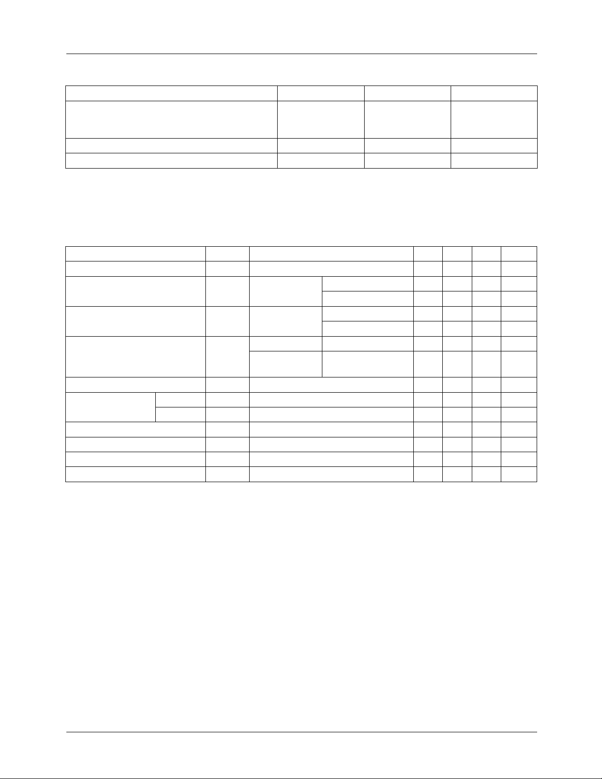
Internal Block Diagram
V
I
3
2
GND
V
0
1
I
R
SC
REFERE NCE VOLT AGE
SHORT CIRCUIT
PROTECTION
THERMAL SHUTDOWN
CIRCUIT
+
-
Inpu
t
Outpu
t
MC78LXXA/LM78LXXA/MC78L05AA
3-Terminal 0.1A Positive Voltage Regulator
MC78LXXA/LM78LXXA/MC78L05AA
2
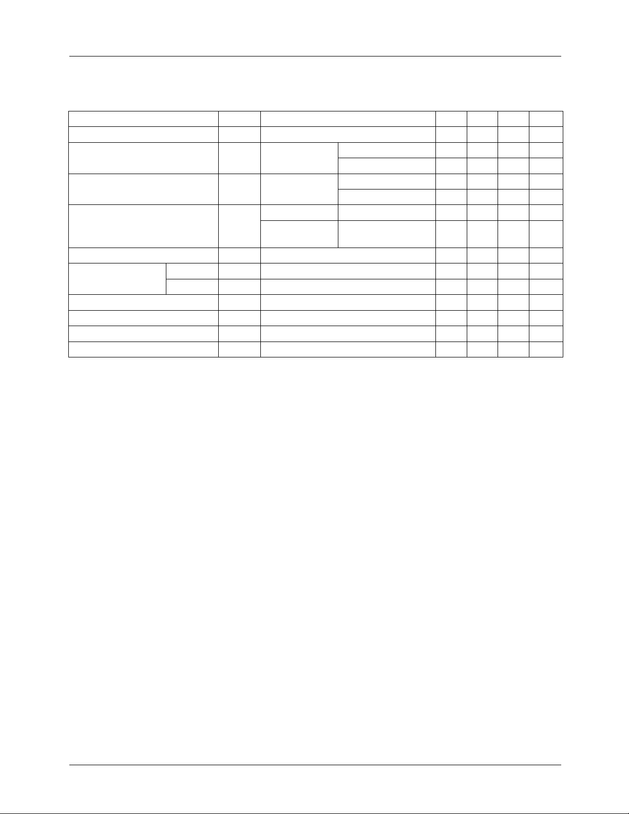
Absolute Maximum Ratings
Electrical Characteristics(MC78L05A/LM78L05A)
(V
I
= 10V, I
O
= 40mA, 0°C
≤ T
J
≤ 125°C, C
I
= 0.33µF, C
O
= 0.1µF, unless otherwise specified. (Note 1)
Note:
1. The max imum st eady sta te usable output cu rrent and inpu t voltage are very depende nt on the heat si nking an d/or lead length
of the package. The data a bove rep resent p ulse tes t conditi ons with junction temper ature as indicate d at the initiatio n of test s.
2. Power dissipation P
D
≤ 0.75W.
Parameter Symbol Value Unit
Input Voltage (for V
O
= 5V, 8V)
(for V
O
= 12V to 18V)
(for V
O
=
24V)
V
I
30
35
40
V
V
V
Operating Junction Temperature Range T
J
0 ~ +150 °C
Storage Temperature Range T
STG
-65 ~ +150 °C
Parameter Symbol Conditions Min. Typ. Max. Unit
Output Voltage V
O
T
J
= 25°C4.85.05.2V
Line Regulation (Note1)
∆V
O
T
J
= 25°C
7V ≤
≤≤
≤ V
I
≤
≤≤
≤ 20V - 8 150 mV
8V ≤
≤≤
≤ V
I
≤
≤≤
≤ 20V - 6 100 mV
Load Regulation (Note1)
∆V
O
T
J
= 25°C
1mA ≤ I
O
≤ 100mA - 11 60 mV
1mA ≤ I
O
≤ 40mA - 5.0 30 mV
Output Voltage V
O
7V ≤ V
I
≤ 20V 1mA ≤ I
O
≤ 40mA - - 5.25 V
7V ≤ V
I
≤ V
MAX
(Note 2)
1mA ≤ I
O
≤ 70mA 4.75 - 5.25 V
Quiescent Current I
Q
T
J
= 25°C-2.05.5mA
Quiescent Current
Change
With Line ∆I
Q
8V ≤V
I
≤ 20V - - 1.5 mA
With Load ∆I
Q
1mA ≤ I
O
≤ 40
mA - - 0.1 mA
Output Noise Voltage V
N
T
A
= 25°C, 10Hz ≤ f ≤ 100kHz - 40 - µV/Vo
Temperature Coefficient of V
O
∆V
O
/∆TI
O
= 5mA - -0.65 - mV/°C
Ripple Rejection RR f = 120Hz, 8V ≤ V
I
≤ 18V, T
J
= 25°C4180 - dB
Dropout Voltage V
D
T
J
= 25°C-1.7-V
MC78LXXA/LM78LXXA/MC78L05AA
3
Electrical Characteristics(MC78L08A)
(Continued)
(V
I
= 14V, I
O
= 40mA, 0°C ≤ T
J
≤ 125°C, C
I
= 0.33µF, C
O
= 0.1µF, unless otherwise specified. (Note 1)
Note:
1. The ma ximum ste ady stat e usable output curre nt and input vo ltage ar e very d epende nt on th e heat s inking a nd/or lead le ngth
of the package. The dat a above repres ent pulse test c onditions with junction temp erature as ind icated at the initi ation of tests.
2. Power dissipation P
D
≤ 0.75W.
Parameter Symbol Conditions Min. Typ. Max. Unit
Output Voltage V
O
T
J
= 25°C 7.7 8.0 8.3 V
Line Regulation (Note1) ∆V
O
T
J
= 25°C
10.5V ≤ V
I
≤ 23V - 10 175 mV
11V ≤ V
I
≤ 23V - 8 125 mV
Load Regulation (Note1) ∆V
O
T
J
= 25°C1mA ≤ I
O
≤ 100mA - 15 80 mV
1mA ≤ I
O
≤ 40mA - 8.0 40 mV
Output Voltage V
O
10.5V ≤ V
I
≤ 23V 1mA ≤ I
O
≤ 40mA 7.6 - 8.4 V
10.5V ≤ V
I
≤
V
MAX
(Note 2)
1mA ≤ I
O
≤ 70mA 7.6 - 8.4 V
Quiescent Current I
Q
T
J
= 25°C-2.05.5mA
Quiescent Current
Change
With Line ∆I
Q
11V ≤ V
I
≤ 23V - - 1.5 mA
With Load ∆I
Q
1mA ≤ I
O
≤ 40mA - - 0.1 mA
Output Noise Voltage V
N
T
A
= 25°C, 10Hz ≤ f ≤100kHz - 60 - µV/Vo
Temperature Coefficient of V
O
∆V
O
/∆TI
O
= 5mA - -0.8 - mV/
°C
Ripple Rejection RR f = 120Hz, 11V ≤ V
I
≤ 21V, T
J
= 25°C39 70 - dB
Dropout Voltage V
D
T
J
= 25°C-1.7-V
MC78LXXA/LM78LXXA/MC78L05AA
4
Electrical Characteristics(MC78L12A/LM78L12A)
(Continued)
(V
I
= 19V, I
O
= 40mA, 0°C ≤ T
J
≤ 125°C, C
I
= 0.33 µF, C
O
= 0.1µF, unless otherwise specified. (Note 1)
Note:
1. The ma ximum ste ady stat e usable output curre nt and input vo ltage ar e very d epende nt on th e heat s inking a nd/or lead le ngth
of the package. The dat a above repres ent pulse test c onditions with junction temp erature as ind icated at the initi ation of tests.
2. Power dissipation P
D
≤ 0.75W.
Parameter Symbol Conditions Min. Typ. Max. Unit
Output Voltage V
O
T
J
= 25°C 11.5 12 12.5 V
Line Regulation (Note1) ∆V
O
T
J
= 25°C
14.5V ≤ V
I
≤ 27V - 20 250 mV
16V ≤ V
I
≤ 27V - 15 200 mV
Load Regulation (Note1) ∆V
O
T
J
= 25°C
1mA ≤ I
O
≤ 100mA - 20 100 mV
1mA ≤ I
O
≤ 40mA - 10 50 mV
Output Voltage V
O
14.5V ≤ V
I
≤ 27V 1mA ≤ I
O
≤ 40mA 11.4 - 12.6 V
14.5V ≤ V
I
≤
V
MAX
(Note 2)
1mA ≤ I
O
≤ 70mA 11.4 - 12.6 V
Quiescent Current I
Q
T
J
= 25°C-2.16.0mA
Quiescent Current
Change
With Line ∆I
Q
16V ≤ V
I
≤ 27V - - 1.5 mA
With Load ∆I
Q
1mA ≤ I
O
≤ 40mA - - 0.1 mA
Output Noise Voltage V
N
T
A
= 25°C, 10Hz ≤ f ≤ 100kHz - 80 - µV/Vo
Temperature Coefficient of V
O
∆V
O
/∆TI
O
= 5mA - -1.0 - mV/°C
Ripple Rejection RR f = 120Hz, 15V ≤ V
I
≤ 25V, T
J
= 25°C37 65 - dB
Dropout Voltage V
D
T
J
= 25°C-1.7-V
MC78LXXA/LM78LXXA/MC78L05AA
5
Electrical Characteristics(MC78L15A)
(Continued)
(V
I
= 23V, I
O
= 40mA, 0°C ≤ T
J
≤ 125°C, C
I
= 0.33 µF, C
O
= 0.1µF, unless otherwise specified. (Note 1)
Note:
1. The maximum s tea dy state usable output cur re nt and input voltage are very dependent on the heat sinking and/or le ad le ngth
of the package. The data a bove rep resent p ulse tes t conditi ons with junction temper ature as indicate d at the initiatio n of test s.
2. Power dissipation P
D
≤ 0.75W.
Parameter Symbol Conditions Min. Typ. Max. Unit
Output Voltage V
O
T
J
= 25°C 14.4 15 15.6 V
Line Regulation (Note1) ∆V
O
T
J
= 25°C
17.5V ≤ V
I
≤ 30V - 25 300 mV
20V ≤ V
I
≤ 30V - 20 250 mV
Load Regulation (Note1) ∆V
O
T
J
= 25°C
1mA ≤ I
O
≤ 100mA - 25 150 mV
1mA ≤ I
O
≤ 40mA - 12 75 mV
Output Voltage V
O
17.5V ≤ V
I
≤ 30V 1mA ≤ I
O
≤ 40mA 14.25 - 15.75 V
17.5V ≤ V
I
≤
V
MAX
(Note 2)
1mA ≤ I
O
≤ 70mA 14.25 - 15.75 V
Quiescent Current I
Q
T
J
= 25°C-2.16.0mA
Quiescent Current
Change
With Line ∆I
Q
20V ≤ V
I
≤ 30V - - 1.5 mA
With Load ∆I
Q
1mA ≤ I
O
≤ 40mA - - 0.1 mA
Output Noise Voltage V
N
T
A
= 25°C, 10Hz ≤ f ≤ 100kHz - 90 - µV/Vo
Temperature Coefficient of V
O
∆V
O
/∆TI
O
= 5mA - -1.3 - mV/°C
Ripple Rejection RR f = 120Hz, 18.5V≤V
I
≤28.5V, T
J
= 25°C34 60 - dB
Dropout Voltage V
D
T
J
= 25°C-1.7-V
 Loading...