


August 1999
Revised October 1999
74ACT16244
16-Bit Buffer/Line Driver with 3-STATE Outputs
General Description
The ACT16244 contains sixteen non-inverting buffers with 3-STATE outputs designed to be employed as a memory and address driver, clock driver, or bus oriented transmitter/receiver. The device is nibble controlled. Each nibble has separate 3-STATE control inputs which can be shorted together for full 16-bit operation.
Features
■Separate control logic for each byte and nibble
■16-bit version of the ACT244
■Outputs source/sink 24 mA
■TTL-compatible inputs
Ordering Code:
Order Number |
Package Number |
Package Description |
|
|
|
74ACT16244SSC |
MS48A |
48-Lead Small Shrink Outline Package (SSOP), JEDEC MO-118, 0.300” Wide |
|
|
|
74ACT16244MTD |
MTD48 |
48-Lead Thin Shrink Small Outline Package (TSSOP), JEDEC MO-153, 6.1mm Wide |
|
|
|
Device also available in Tape and Reel. Specify by appending suffix letter “X” to the ordering code.
Logic Symbol |
Connection Diagram |
Pin Description
Pin Names |
Description |
||
|
|
|
|
|
|
n |
Output Enable Input (Active LOW) |
|
OE |
||
|
I0–I15 |
Inputs |
|
|
O0–O15 |
Outputs |
|
|
|
|
|
FACTä is a trademark of Fairchild Semiconductor Corporation.
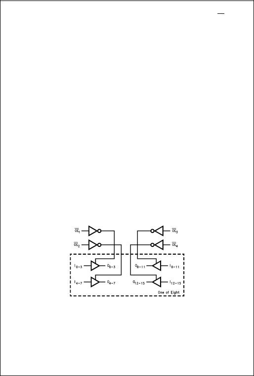
Outputs STATE-3 with Driver Buffer/Line Bit-16 74ACT16244
© 1999 Fairchild Semiconductor Corporation |
DS500295 |
www.fairchildsemi.com |
74ACT16244
Functional Description
The ACT16244 contains sixteen non-inverting buffers with |
puts are controlled by an Output Enable (OEn) input for |
|||||
3-STATE standard outputs. The device is nibble (4 bits) |
each nibble. When |
OE |
n is LOW, the outputs are in 2-state |
|||
controlled with each nibble functioning identically, but inde- |
|
|
|
|
|
|
mode. When OEn is HIGH, the outputs are in the high |
||||||
pendent of the other. The control pins can be shorted |
||||||
impedance mode, but this does not interfere with entering |
||||||
together to obtain full 16-bit operation. The 3-STATE out- |
||||||
new data into the inputs. |
||||||
|
||||||
Truth Tables
|
|
|
Inputs |
Outputs |
|
|
|
|
|
|
|
|
I0–I 3 |
O0–O 3 |
|
OE1 |
|||
|
L |
L |
L |
|
|
L |
H |
H |
|
|
H |
X |
Z |
|
|
|
|
|
|
|
|
|
|
|
|
|
|
Inputs |
Outputs |
|
|
|
|
|
|
|
|
I8–I 11 |
O8–O 11 |
|
OE3 |
|||
|
L |
L |
L |
|
|
L |
H |
H |
|
|
H |
X |
Z |
|
|
|
|
|
|
H = HIGH Voltage Level
L = LOW Voltage Level
X = Immaterial
Z = High Impedance
|
|
|
Inputs |
|
Outputs |
|
|
|
|
||
|
|
|
I4–I |
|
O4–O 7 |
OE2 |
7 |
||||
|
L |
L |
|
L |
|
|
L |
H |
H |
||
|
H |
X |
|
Z |
|
|
|
|
|
|
|
|
|
|
|
|
|
|
|
|
Inputs |
|
Outputs |
|
|
|
|
||
|
|
|
I12–I |
|
O12–O 15 |
OE4 |
15 |
||||
|
L |
L |
|
L |
|
|
L |
H |
H |
||
|
H |
X |
|
Z |
|
|
|
|
|
|
|
Logic Diagram
www.fairchildsemi.com |
2 |

Absolute Maximum Ratings(Note 1)
Supply Voltage (VCC) |
−0.5V to +7.0V |
DC Input Diode Current (IIK) |
|
VI = − 0.5V |
−20 mA |
VI = VCC + 0.5V |
+20 mA |
DC Output Diode Current (IOK) |
|
VO = −0.5V |
−20 mA |
VO = VCC + 0.5V |
+20 mA |
DC Output Voltage (VO) |
−0.5V to VCC + 0.5V |
DC Output Source/Sink Current (IO) |
±50 mA |
DC VCC or Ground Current |
|
per Output Pin |
±50 mA |
Junction Temperature |
+140°C |
Storage Temperature |
−65°C to +150°C |
Recommended Operating
Conditions
Supply Voltage (VCC) |
4.5V to 5.5V |
Input Voltage (VI) |
0V to VCC |
Output Voltage (VO) |
0V to VCC |
Operating Temperature (TA) |
−40°C to +85°C |
Minimum Input Edge Rate ( V/ t) |
125 mV/ns |
VIN from 0.8V to 2.0V |
|
VCC @ 4.5V, 5.5V |
|
Note 1: Absolute maximum ratings are those values beyond which damage to the device may occur. The databook specifications should be met, without exception to ensure that the system design is reliable over its power supply, temperature, and output/input loading variables. Fairchild does not recommend operation of FACTä circuits outside databook specifications.
DC Electrical Characteristics
Symbol |
Parameter |
VCC |
TA = +25°C |
TA = −40°C to +85°C |
Units |
Conditions |
||
|
|
(V) |
Typ |
Guaranteed Limits |
|
|
|
|
|
|
|
|
|
|
|
|
|
VIH |
Minimum HIGH Input Voltage |
4.5 |
1.5 |
2.0 |
2.0 |
V |
VOUT = 0.1V |
|
|
|
5.5 |
1.5 |
2.0 |
2.0 |
or VCC − 0.1V |
||
|
|
|
||||||
VIL |
Maximum LOW Input Voltage |
4.5 |
1.5 |
0.8 |
0.8 |
V |
VOUT = 0.1V |
|
|
|
5.5 |
1.5 |
0.8 |
0.8 |
or VCC − 0.1V |
||
|
|
|
||||||
VOH |
Minimum HIGH Output Voltage |
4.5 |
4.49 |
4.4 |
4.4 |
V |
IOUT = −50 μA |
|
|
|
5.5 |
5.49 |
5.4 |
5.4 |
|||
|
|
|
|
|
||||
|
|
|
|
|
|
|
|
|
|
|
|
|
|
|
|
VIN = VIL or VIH |
|
|
|
4.5 |
|
3.86 |
3.76 |
V |
IOH = −24 mA |
|
|
|
5.5 |
|
4.86 |
4.76 |
|
IOH = −24 mA (Note 2) |
|
VOL |
Maximum LOW Output Voltage |
4.5 |
0.001 |
0.1 |
0.1 |
V |
IOUT = 50 μA |
|
|
|
5.5 |
0.001 |
0.1 |
0.1 |
|||
|
|
|
|
|
||||
|
|
|
|
|
|
|
|
|
|
|
|
|
|
|
|
VIN = VIL or VIH |
|
|
|
4.5 |
|
0.36 |
0.44 |
V |
IOH = 24 mA |
|
|
|
5.5 |
|
0.36 |
0.44 |
|
IOH = 24 mA (Note 2) |
|
IOZ |
Maximum 3-STATE Leakage Current |
5.5 |
|
± 0.5 |
± 5.0 |
μA |
VI = VIL, VIH |
|
|
|
|
|
|
|
|
VO = VCC, GND |
|
IIN |
Maximum Input Leakage Current |
5.5 |
|
± 0.1 |
± 1.0 |
μA |
VI = VCC, GND |
|
ICCT |
Maximum ICC/Input |
5.5 |
0.6 |
|
1.5 |
mA |
VI = VCC −2.1V |
|
ICC |
Max Quiescent Supply Current |
5.5 |
|
8.0 |
80.0 |
μA |
VIN = VCC or GND |
|
IOLD |
Minimum Dynamic |
5.5 |
|
|
75 |
mA |
VOLD = 1.65V Max |
|
IOHD |
Output Current (Note 3) |
|
|
−75 |
mA |
VOHD = 3.85V Min |
||
|
|
|
||||||
Note 2: All outputs loaded; thresholds associated with output under test.
Note 3: Maximum test duration 2.0 ms; one output loaded at a time.
74ACT16244
3 |
www.fairchildsemi.com |
 Loading...