


74ACT16240SSCX
© 1999 Fairchild Semiconductor Corporation DS500293 www.fairchildsemi.com
August 1999
Revised October 1999
74ACT16240 16-Bit Inverting Buffer/Line Driver with 3-STATE Outputs
74ACT16240
16-Bit Inverting Buffer/Line Driver with 3-STATE Outputs
General Description
The ACT16240 contain s sixteen inverting buffers with 3STATE outputs designed to be employed as a memory and
address driver, clock driver, or bus-oriented transmitter/
receiver. The device is nibble controlled. Each nibble has
separate 3-STATE control inputs which can be shorted
together for full 16-bit operation.
Features
■ Separate control logic for each byte
■ 16-bit version of the ACT240
■ Outputs source/sink 24 mA
■ TTL-compatible inputs
Ordering Code:
Device also available in Tape and Reel. Specify by appending s uffix let te r “X” to the ordering code.
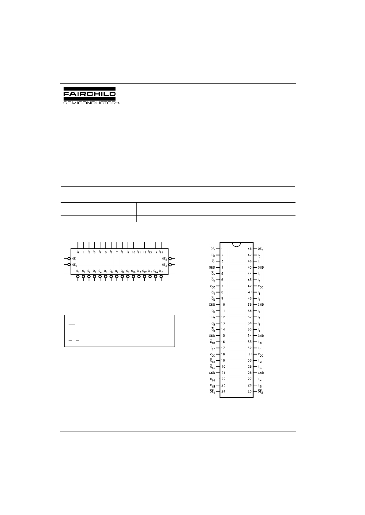
Logic Symbol
Pin Descriptions
Connection Diagram
FACT is a trade m ark of F airchild Semicondu ctor Corporation.
Order Number Package Number Package Description
74ACT16240SSC MS48A 48-Lead Small Shrink Outline Package (SSOP), JEDEC MO-118, 0.300” Wide
74ACT16240MTD MTD48 48-Lead Thin Shrink Small Outline Package (TSSOP), JEDEC MO-153, 6.1mm Wide
Pin Names Description
OE
n
Output Enable Inputs (Active LOW)
I
0–I15
Inputs
O
0–O15
Outputs
www.fairchildsemi.com 2
74ACT16240
Truth Tables
H = HIGH Voltage Level
L = LOW Voltage Level
X = Immaterial
Z = High Impedance
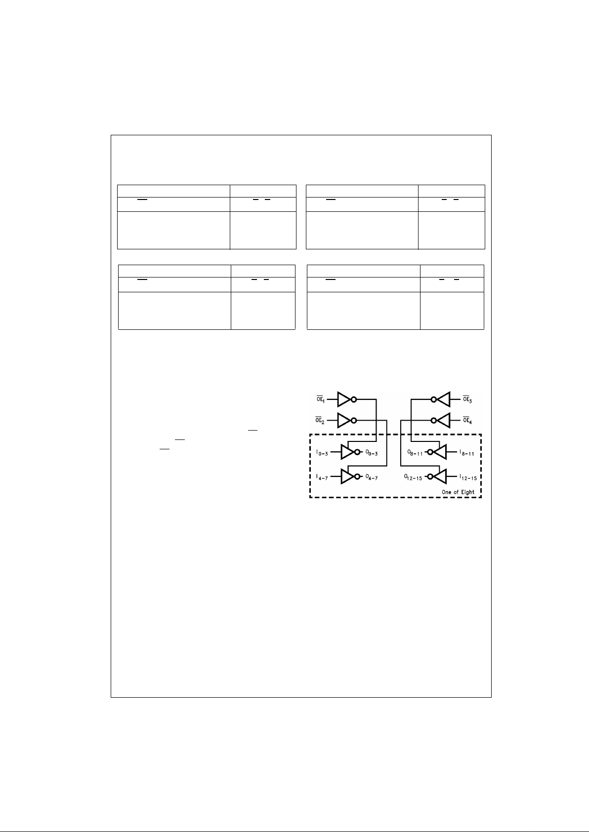
Functional Description
The ACT16240 contains sixteen inverting buffers with 3STATE standar d outputs. Th e device is n ibb le (4 bits) controlled with each nibble fun cti on ing ide nti ca lly, but independently of the other. The control pins may be shorted
together to obtain full 16-bit operation. The 3-STATE ou tputs are controlled by an Output Enable (OE
n
) input for
each nibble. When OE
n
is LOW, the outputs are in 2-state
mode. When OE
n
is HIGH, the outputs are in the high
impedance mode, but this doe s not interfere with enterin g
new data into the inputs.
Logic Diagram
Inputs Outputs
OE
1
I0–I
3
O0–O
3
LL H
LH L
HX Z
Inputs Outputs
OE
2
I4–I
7
O4–O
7
LL H
LH L
HX Z
Inputs Outputs
OE
3
I8–I
11
O8–O
11
LL H
LH L
HX Z
Inputs Outputs
OE
4
I12–I
15
O12–O
15
LL H
LH L
HX Z
3 www.fairchildsemi.com
74ACT16240
Absolute Maximum Ratings(Note 1) Recommended Operating
Conditions
Note 1: Absolute maximum ratings are those values beyond which damage
to the device may occur. The databook specifications should be met, without exception to ensure that the system design is reliable over its power
supply, temperature, and ou tput/inp ut load ing vari ables. Fairchild does n ot
recommend operat ion of FACT circuits outside da t abook specifications.
DC Electrical Characteristics
Note 2: All outputs loaded; thresholds assoc iated with output under t es t .
Note 3: Maximum test duration 2.0 ms; one output loaded at a time.
Supply Voltage (VCC) −0.5V to +7.0V
DC Input Diode Current (I
IK
)
V
I
= −0.5V −20 mA
V
I
= VCC + 0.5V +20 mA
DC Output Diode Current (I
OK
)
V
O
= −0.5V −20 mA
V
O
= VCC + 0.5V +20 mA
DC Output Voltage (V
O
) −0.5V to VCC + 0.5V
DC Output Source/Sink Current (I
O
) ± 50 mA
DC V
CC
or Ground Current
per Output Pin ± 50 mA
Junction Temperature +140°C
Storage Temperature −65°C to +150°C
Supply Voltage (V
CC
) 4.5V to 5.5V
Input Voltage (V
I
)0V to V
CC
Output Voltage (VO)0V to V
CC
Operating Temperature (TA) −40°C to +85°C
Minimum Input Edge Rate (∆V/∆t) 125 mV/ns
V
IN
from 0.8V to 2.0V
V
CC
@ 4.5V, 5.5V
Symbol Parameter
V
CC
TA = +25°C
TA = −40°C to +85°C
Units Conditions
(V) Typ Guaranteed Limits
V
IH
Minimum HIGH 4.5 1.5 2.0 2.0
V
V
OUT
= 0.1V
Input Voltage 5.5 1.5 2.0 2.0 or VCC − 0.1V
V
IL
Maximum LOW 4.5 1.5 0.8 0.8
V
V
OUT
= 0.1V
Input Voltage 5.5 1.5 0.8 0.8 or VCC − 0.1V
V
OH
Minimum HIGH 4.5 4.49 4.4 4.4
VI
OUT
= −50 µA
Output Voltage 5.5 5.49 5.4 5.4
VIN = VIL or V
IH
4.5 3.86 3.76 V IOH = −24 mA
5.5 4.86 4.76 IOH = −24 mA (Note 2)
V
OL
Maximum LOW 4.5 0.001 0.1 0.1
VI
OUT
= 50 µA
Output Voltage 5.5 0.001 0.1 0.1
VIN = VIL or V
IH
4.5 0.36 0.44 V IOL = 24 mA
5.5 0.36 0.44 IOL = 24 mA (Note 2)
I
OZ
Maximum 3-STATE
5.5 ±0.5 ±5.0 µA
VI = VIL, V
IH
Leakage Current VO = VCC, GND
I
IN
Maximum Input Leakage Current 5.5 ± 0.1 ± 1.0 µAVI = VCC, GND
I
CCT
Maximum ICC/Input 5.5 0.6 1.5 mA VI = VCC − 2.1V
I
CC
Max Quiescent Supply Current 5.5 8.0 80.0 µAVIN = VCC or GND
I
OLD
Minimum Dynamic
5.5
75 mA V
OLD
= 1.65V Max
I
OHD
Output Current (Note3) −75 mA V
OHD
= 3.85V Min
 Loading...