


AD1555 |
|
a |
24-Bit - ADC |
with Low Noise PGA |
FEATURES AD1555
Fourth Order - Modulator
Large Dynamic Range
116 dB Min, 120 dB Typical @ 1 ms
117 dB Typical @ 0.5 ms
Low Input Noise: 80 nV rms @ 4 ms with Gain of 34,128
Low Distortion: –111 dB Max, –120 dB Typical Low Intermodulation: 122 dB
Sampling Rate at 256 kSPS
Very High Jitter Tolerance
No External Antialias Filter Required Programmable Gain Front End
Input Range: 2.25 V
Robust Inputs
Gain Settings: 1, 2.5, 8.5, 34, 128 Common-Mode Rejection (DC to 1 kHz)
93 dB Min, 101 dB Typical @ Gain of 1 77 mW Typical Low Power Dissipation Standby Modes
AD1556
FIR Digital Filter/Decimator
Serial or Parallel Selection of Configuration Output Word Rates: 250 SPS to 16 kSPS 6.2 mW Typ Low Power Dissipation
70 W in Standby Mode
Reference Design and Evaluation Board with Software Available
APPLICATIONS
Seismic Data Acquisition Systems
Chromatography
Automatic Test Equipment
GENERAL DESCRIPTION
The AD1555 is a complete sigma-delta modulator, combined with a programmable gain amplifier intended for low frequency,
AD1555/AD1556
high dynamic range measurement applications. The AD1555 outputs a ones-density bitstream proportional to the analog input. When used in conjunction with the AD1556 digital filter/ decimator, a high performance ADC is realized.
The continuous-time analog modulator input architecture avoids the need for an external antialias filter. The programmable gain front end simplifies system design, extends the dynamic range, and reduces the system board area. Low operating power and standby modes makes the AD1555 ideal for remote battery-pow- ered data acquisition systems.
The AD1555 is fabricated on Analog DevicesÕ BiCMOS process that has high performance bipolar devices along with CMOS transistors. The AD1555 and AD1556 are packaged, respectively, in 28-lead PLCC and 44-lead MQFP packages and are specified from Ð55°C to +85°C (AD1556 and AD1555 B Grade) and from 0°C to 85°C (AD1555 A Grade).
|
0 |
|
|
|
|
|
|
|
|
|
|
|
|
|
–20 |
|
|
|
|
|
|
|
|
fIN = 24.4Hz |
|
||
|
|
|
|
|
|
|
|
|
SNR = 116.7dB |
|
|||
|
|
|
|
|
|
|
|
|
|
||||
|
–40 |
|
|
|
|
|
|
|
|
THD = –120.6dB |
|
||
|
|
|
|
|
|
|
|
|
|
|
|
|
|
– dBr |
–60 |
|
|
|
|
|
|
|
|
|
|
|
|
|
|
|
|
|
|
|
|
|
|
|
|
||
–80 |
|
|
|
|
|
|
|
|
|
|
|
|
|
|
|
|
|
|
|
|
|
|
|
|
|
||
AMPLITUDE |
–100 |
|
|
|
|
|
|
|
|
|
|
|
|
|
|
|
|
|
|
|
|
|
|
|
|
|
|
|
–120 |
|
|
|
|
|
|
|
|
|
|
|
|
|
|
|
|
|
|
|
|
|
|
|
|
|
|
|
–140 |
|
|
|
|
|
|
|
|
|
|
|
|
|
|
|
|
|
|
|
|
|
|
|
|
|
|
|
–160 |
|
|
|
|
|
|
|
|
|
|
|
|
|
|
|
|
|
|
|
|
|
|
|
|
|
|
|
–180 |
|
|
|
|
|
|
|
|
|
|
|
|
|
|
|
|
|
|
|
|
|
|
|
|
|
|
|
–200 |
|
|
|
|
|
|
|
|
|
|
|
|
|
|
|
|
|
|
|
|
|
|
|
|
|
|
0 |
50 |
100 |
150 |
200 |
250 |
300 |
350 |
400 |
450 |
500 |
FREQUENCY – Hz
Figure 1. FFT Plot, Full-Scale AIN Input, Gain of 1
FUNCTIONAL BLOCK DIAGRAM
|
|
REFIN |
REFCAP2 |
REFCAP1 |
AGND3 |
|
|
|
|
|
|
|
MODE CONTROL |
|
|
REF DIVIDER |
|
|
LOGIC |
|
|
|
|
|
DAC |
|
OVERVOLTAGE |
|
|
|
|
|
DETECTION |
|
|
|
|
|
|
|
|
|
|
PGA |
|
LOOP |
|
|
|
|
|
|
|
||
AIN (+) |
MUX |
|
|
FILTER |
|
|
|
|
|
|
|
||
AIN (–) |
|
|
|
|
|
|
TIN (+) |
|
|
|
|
|
CLOCK |
TIN (–) |
|
|
|
AD1555 |
GENERATION |
|
|
|
|
|
|||
|
AGND1 |
PGAOUT |
MODIN AGND2 +VA |
–VA |
VL DGND |
|
REV. B
|
PGA0...PGA4 |
H/S |
ERROR |
|
|
CB0...CB4 |
PGA |
CONFIGURATION |
INPUT SHIFT |
|
|
|
DIN |
||||
|
CONTROL |
REGISTER |
REGISTER |
||
|
|
||||
MFLG |
|
|
|
|
SCLK |
|
|
STATUS |
|
CS |
|
|
|
|
|
||
|
|
|
REGISTER |
|
R/W |
CSEL |
|
|
|
|
|
|
|
|
DATA |
|
|
|
INPUT |
DIGITAL |
|
DOUT |
|
TDATA |
|
OUTPUT |
|||
MUX |
FILTER |
|
|||
|
|
MUX |
|
||
|
|
|
|
|
|
MDATA |
|
|
DATA |
|
DRDY |
|
|
|
|
|
|
|
CLOCK DIVIDER |
REGISTER |
|
RSEL |
|
MCLK |
AD1556 |
|
|||
|
|
|
|||
|
|
|
|
||
|
CLKIN SYNC |
BW0...BW2 RESET PWRDN GND |
VL |
||
Information furnished by Analog Devices is believed to be accurate and reliable. However, no responsibility is assumed by Analog Devices for its use, nor for any infringements of patents or other rights of third parties that may result from its use. No license is granted by implication or otherwise under any patent or patent rights of Analog Devices.
One Technology Way, P.O. Box 9106, Norwood, MA 02062-9106, U.S.A.
Tel: 781/329-4700 |
www.analog.com |
Fax: 781/326-8703 |
© Analog Devices, Inc., 2002 |
AD1555/AD1556
AD1555–SPECIFICATIONS
(+VA = +5 V; –VA = –5 V; VL = 5 V; AGND = DGND = 0 V; MCLK = 256 kHz; TA = TMIN to TMAX, unless otherwise noted.)
|
|
AD1555BP |
|
AD1555AP |
|
|
||
Parameter |
Notes |
Min |
Typ |
Max |
Min |
Typ |
Max |
Unit |
|
|
|
|
|
|
|
|
|
PGA Gain Settings |
1, 2.5, 8.5, 34, 128 |
|
|
|
|
|
|
|
|
|
|
|
|
|
|
|
|
AC ACCURACY |
|
|
|
|
|
|
|
|
Dynamic Range1 |
PGA Gain of 1 |
116.5 |
120 |
|
116 |
120 |
|
dB |
|
PGA Gain of 2.5 |
116 |
119.5 |
|
115.5 |
119.5 |
|
dB |
|
PGA Gain of 8.5 |
114 |
117.5 |
|
114 |
117.5 |
|
dB |
|
PGA Gain of 34 |
104.5 |
109.5 |
|
104.5 |
109.5 |
|
dB |
Total Harmonic Distortion2 |
PGA Gain of 128 |
|
98 |
|
|
98 |
|
dB |
PGA Gain of 1 |
|
Ð120 |
Ð111 |
|
Ð120 |
Ð107 |
dB |
|
|
PGA Gain of 2.5 |
|
Ð116 |
Ð108 |
|
Ð116 |
Ð107 |
dB |
|
PGA Gain of 8.5 |
|
Ð116 |
Ð106 |
|
Ð116 |
Ð105 |
dB |
|
PGA Gain of 34 |
|
Ð115 |
Ð101 |
|
Ð115 |
Ð101 |
dB |
Jitter Tolerance3 |
PGA Gain of 128 |
|
Ð108 |
|
|
Ð108 |
|
dB |
|
|
|
300 |
|
|
300 |
ps |
|
Intermodulation Distortion4 |
PGA Gain of 1 |
|
122 |
|
|
122 |
|
dB |
DC ACCURACY |
|
|
|
|
|
|
|
|
Absolute Gain Error5 |
PGA Gain of 1, 2.5 |
Ð3.5 |
|
+3.5 |
Ð3.5 |
|
+3.5 |
% |
|
PGA Gain of 8.5 |
Ð4.5 |
|
+4.5 |
Ð4.5 |
|
+4.5 |
% |
|
PGA Gain of 34 |
Ð10 |
|
+10 |
Ð10 |
|
+10 |
% |
Gain Stability Over Temperature5 |
|
|
± 15 |
|
|
± 15 |
|
ppm/°C |
Offset5, 6 |
All PGA Gain |
|
Ð60 |
|
|
Ð60 |
|
mV |
Offset Drift5, 6 |
|
|
6 |
|
|
6 |
|
µV/°C |
ANALOG INPUT |
|
|
|
± 2.25 |
|
|
± 2.25 |
|
Full-Scale Nondifferential Input |
MODIN |
|
|
|
|
V |
||
Input Impedance |
MODIN |
|
20 |
± 2.25 |
|
20 |
± 2.25 |
k |
Full-Scale Differential Input |
PGA Gain of 1 |
|
|
|
|
V |
||
|
Other PGA Gain Settings |
|
See Table I |
See Table I |
|
MΩ |
||
Differential Input Impedance |
AIN, TIN Inputs |
|
140 |
± 2.25 |
|
140 |
± 2.25 |
|
Common-Mode Range |
VCM = ± 2.25 V, fIN = 200 Hz |
|
|
|
|
V |
||
Common-Mode Rejection Ratio |
|
|
|
|
|
|
|
|
|
PGA Gain of 1 |
93 |
101 |
|
91 |
101 |
|
dB |
|
PGA Gain of 2.5 |
95 |
102 |
|
91.5 |
102 |
|
dB |
|
PGA Gain of 8.5, 34 |
95.5 |
108 |
|
94.5 |
108 |
|
dB |
Power Supply Rejection Ratio7 |
PGA Gain of 128 |
|
108 |
|
|
108 |
|
dB |
|
|
50 |
|
|
50 |
|
dB |
|
AIN to TIN Crosstalk Isolation |
fIN = 200 Hz |
|
130 |
|
|
130 |
|
dB |
Differential Input Current |
|
|
130 |
|
|
130 |
|
nA |
|
|
|
|
|
|
|
|
|
TEMPERATURE RANGE8 |
|
|
|
|
|
|
|
°C |
Specified Performance |
TMIN to TMAX |
Ð55 |
|
+85 |
0 |
|
85 |
|
REFERENCE INPUT9 |
|
|
|
|
|
|
|
|
Input Voltage Range |
|
2.990 |
3.0 |
3.010 |
2.990 |
3.0 |
3.010 |
V |
Input Current |
|
|
130 |
|
|
130 |
|
µA |
|
|
|
|
|
|
|
|
|
DIGITAL INPUTS OUTPUTS |
|
|
|
|
|
|
|
|
VIL |
|
Ð0.3 |
|
+0.8 |
Ð0.3 |
|
+0.8 |
V |
VIH |
|
2.0 |
|
VL + 0.3 |
2.0 |
|
VL + 0.3 |
V |
IIL |
|
Ð10 |
|
+10 |
Ð10 |
|
+10 |
µA |
IIH |
|
Ð10 |
|
+10 |
Ð10 |
|
+10 |
µA |
VOL |
ISINK = +2 mA |
|
|
0.4 |
|
|
0.4 |
V |
VOH |
ISOURCE = Ð2 mA |
2.4 |
|
|
2.4 |
|
|
V |
–2– |
REV. B |
AD1555/AD1556
|
|
|
AD1555BP |
|
|
AD1555AP |
|
|
Parameter |
Notes |
Min |
Typ |
Max |
Min |
Typ |
Max |
Unit |
|
|
|
|
|
|
|
|
|
POWER SUPPLIES |
|
|
|
|
|
|
|
|
Recommended Operating Conditions |
|
|
|
|
|
|
|
|
+VA |
|
4.75 |
5 |
5.25 |
4.75 |
5 |
5.25 |
V |
ÐVA |
|
Ð5.25 |
Ð5 |
Ð4.75 |
Ð5.25 |
Ð5 |
Ð4.75 |
V |
VL |
|
4.75 |
5 |
5.25 |
4.75 |
5 |
5.25 |
V |
Quiescent Currents |
|
|
|
|
|
|
|
|
I(+VA)10 |
|
|
8 |
10 |
|
8 |
10 |
mA |
I(ÐVA)10 |
|
|
8 |
9.5 |
|
8 |
9.5 |
mA |
I(VL) |
|
|
30 |
42 |
|
30 |
42 |
A |
Power Dissipation10 |
PGA in Standby Mode11 |
|
77 |
96 |
|
77 |
96 |
mW |
|
|
56 |
70 |
|
56 |
70 |
mW |
|
|
In Power-Down Mode11, 12 |
|
|
|
|
|
|
W |
|
Reference Input = 3 V |
|
650 |
|
|
650 |
|
|
|
Reference Input = 0 V |
|
250 |
|
|
250 |
|
W |
NOTES
1Tested at the output word rate FO = 1 kHz. FO is the AD1556 output word rate, the inverse of the sampling rate. See Tables I, Ia, Ib for other output word rates.
2Tested with a full-scale input signal at approximately 24 Hz. 3This parameter is guaranteed by design.
4Tested at the output word rate FO = 1 kHz with input signals of 30 Hz and 50 Hz, each 6 dB down full scale.
5This specification is for the AD1555 only and does not include the errors from external components as, for instance, the external reference. 6This offset specification is referred to the modulator output.
7Characterized with a 100 mV p-p sine wave applied separately to each supply. 8Contact factory for extended temperature range.
9Recommended Reference: AD780BR.
10Specified with analog inputs grounded.
11See Table III for configuration conditions.
12Specified with MCLK input grounded.
Specifications subject to change without notice.
AD1556–SPECIFICATIONS (VL = 2.85 V to 5.25 V; CLKIN = 1.024 MHz; TA = TMIN to TMAX unless otherwise noted.)
|
|
|
AD1556AS |
|
|
Parameter |
Notes |
Min |
Typ |
Max |
Unit |
|
|
|
|
|
|
FILTER PERFORMANCES |
|
|
|
|
|
Pass-Band Ripple |
|
Ð0.05 |
|
+0.05 |
dB |
Stop-Band Attenuation |
All Filters Except FO =16 kHz |
|
|
Ð135 |
dB |
Filters Characteristics |
FO =16 kHz |
|
See Table II |
Ð86 |
dB |
|
|
|
|
||
|
|
|
|
|
|
DIGITAL INPUTS OUTPUTS |
|
|
|
|
|
VIL |
|
Ð0.3 |
|
+0.8 |
V |
VIH |
|
+2.0 |
|
VL + 0.3 |
V |
IIL |
|
Ð10 |
|
+10 |
A |
IIH |
|
Ð10 |
|
+10 |
A |
VOL |
ISINK = +2 mA |
|
|
+0.5 |
V |
VOH |
ISOURCE = Ð2 mA |
VL Ð 0.6 |
|
|
V |
POWER SUPPLIES |
|
|
|
|
|
Specified Performance |
|
|
|
|
|
VL |
|
2.85 |
|
5.25 |
V |
Quiescent Currents |
|
|
|
|
|
I(VL) |
|
|
4 |
5 |
mA |
Power Dissipation |
VL = 3.3 V, FO = 1 kHz |
|
6.2 |
8.5 |
mW |
|
In Power-Down Mode |
|
70 |
|
W |
TEMPERATURE RANGE* |
|
|
|
|
°C |
Specified Performance, TMIN to TMAX |
|
Ð55 |
|
+85 |
*Contact factory for extended temperature range.
Specifications subject to change without notice.
REV. B |
–3– |
AD1555/AD1556
Table I. Dynamic and Noise Typical Performances
Input and Gain |
MODIN |
|
PGA = 1 (0 dB) |
PGA = 2.5 (8 dB) |
PGA = 8.5 (19 dB) |
PGA = 34 (31 dB) |
|
PGA = 128 (42 dB) |
|||||
|
|
|
|
|
|
|
|
|
|
|
|
|
|
Input Range |
1.6 V rms |
|
1.6 V rms |
636 mV rms |
187 mV rms |
|
47 mV rms |
|
12.4 mV rms |
||||
Dynamic Range |
|
|
|
|
|
|
|
|
|
|
|
|
|
FO = 16 kHz (1/16 ms) |
40 dB |
|
40 dB |
40 dB |
|
40 dB |
|
40 dB |
|
40 dB |
|||
FO = 8 kHz (1/8 ms) |
69 dB |
|
69 dB |
69 dB |
|
69 dB |
|
69 dB |
|
69 dB |
|||
FO = 4 kHz (1/4 ms) |
98 dB |
|
98 dB |
98 dB |
|
98 dB |
|
97 dB |
|
91 dB |
|||
FO = 2 kHz (1/2 ms) |
117 dB |
|
117 dB |
116.5 dB |
114.5 dB |
|
106.5 dB |
|
95 dB |
||||
FO = 1 kHz (1 ms) |
120 dB |
|
120 dB |
119.5 dB |
117.5 dB |
|
109.5 dB |
|
98 dB |
||||
FO = 500 Hz (2 ms) |
123 dB |
|
123 dB |
122.5 dB |
120 dB |
|
112.5 dB |
|
101 dB |
||||
FO = 250 Hz (4 ms) |
126 dB |
|
126 dB |
125.5 dB |
123 dB |
|
115.5 dB |
|
104 dB |
||||
Equivalent Input Noise |
|
|
|
|
|
|
|
|
|
470 V rms |
|
138 V rms |
|
FO = 16 kHz (1/16 ms) |
15.5 mV rms |
|
15.5 mV rms |
6.17 mV rms |
1.84 mV rms |
|
|
||||||
FO = 8 kHz (1/8 ms) |
560 V rms |
|
560 V rms |
220 V rms |
65.5 V rms |
|
16.4 V rms |
|
4.5 V rms |
||||
FO = 4 kHz (1/4 ms) |
20 V rms |
|
20 V rms |
8 V rms |
2.36 V rms |
|
661 nV rms |
|
351 nV rms |
||||
FO = 2 kHz (1/2 ms) |
2.25 V rms |
|
2.25 V rms |
952 nV rms |
353 nV rms |
|
225 nV rms |
|
223 nV rms |
||||
FO = 1 kHz (1 ms) |
1.59 V rms |
|
1.59 V rms |
674 nV rms |
250 nV rms |
|
159 nV rms |
|
159 nV rms |
||||
FO = 500 Hz (2 ms) |
1.13 V rms |
|
1.13 V rms |
477 nV rms |
187 nV rms |
|
113 nV rms |
|
111 nV rms |
||||
FO = 250 Hz (4 ms) |
797 nV rms |
|
797 nV rms |
338 nV rms |
133 nV rms |
|
80 nV rms |
|
79 nV rms |
||||
|
Table Ia. Minimum Dynamic Performances (AD1555AP Only)* |
|
|
||||||||||
|
|
|
|
|
|
|
|
|
|
|
|
|
|
Input and Gain |
MODIN |
|
PGA = 1 (0 dB) |
|
PGA = 2.5 (8 dB) |
|
PGA = 8.5 (19 dB) |
|
PGA = 34 (31 dB) |
||||
|
|
|
|
|
|
|
|
|
|
|
|
|
|
FO = 1 kHz (1 ms) |
116 |
|
116 |
|
|
115.5 |
|
|
114 |
|
|
104.5 |
|
FO = 500 Hz (2 ms) |
119 |
|
119 |
|
|
118.5 |
|
|
117 |
|
|
107.5 |
|
FO = 250 Hz (4 ms) |
122 |
|
122 |
|
|
121.5 |
|
|
120 |
|
|
110.5 |
|
*Not tested in production. Guaranteed by design.
Table Ib. Minimum Dynamic Performances (AD1555BP Only)*
Input and Gain |
MODIN |
PGA = 1 (0 dB) |
PGA = 2.5 (8 dB) |
PGA = 8.5 (19 dB) |
PGA = 34 (31 dB) |
|
|
|
|
|
|
FO = 1 kHz (1 ms) |
116.5 |
116.5 |
116 |
114 |
104.5 |
FO = 500 Hz (2 ms) |
119.5 |
119.5 |
119 |
117 |
107.5 |
FO = 250 Hz (4 ms) |
122.5 |
122.5 |
121 |
120 |
110.5 |
*Not tested in production. Guaranteed by design.
Table II. Filter Characteristics
Output Word Rate FO |
Pass Band |
–3 dB Frequency |
Stop Band |
Group Delay |
|
(Sampling Rate in ms) |
(Hz) |
(Hz) |
(Hz) |
(ms) |
|
|
|
|
|
|
|
16000 Hz (1/16 ms) |
6000 |
6480 |
8000 |
0.984 |
|
8000 |
Hz (1/8 ms) |
3000 |
3267.5 |
4000 |
3 |
4000 |
Hz (1/4 ms) |
1500 |
1634 |
2000 |
6 |
2000 |
Hz (1/2 ms) |
750 |
816.9 |
1000 |
12 |
1000 |
Hz (1 ms) |
375 |
408.5 |
500 |
24 |
500 Hz (2 ms) |
187.5 |
204.2 |
250 |
48 |
|
250 Hz (4 ms) |
93.75 |
101.4 |
125 |
93 |
|
|
|
|
|
|
|
–4– |
REV. B |
AD1555/AD1556
(+VA = +5 V 5%; –VA = –5 V 5%; AD1555 VL = 5 V 5%, AD1556 VL = 2.85 V to 5.25 V;
TIMING SPECIFICATIONS CLKIN = 1.024 MHz; AGND = DGND = 0 V; CL = 50 pF; TA = TMIN to TMAX, unless otherwise noted)
|
Symbol |
Min |
Typ |
Max |
Unit |
|
|
|
|
|
|
CLKIN Frequency1 |
fCLKIN |
0.975 |
1.024 |
1.075 |
MHz |
CLKIN Duty Cycle Error |
|
45 |
|
55 |
% |
MCLK Output Frequency1 |
|
|
fCLKIN/4 |
|
|
SYNC Setup Time |
t1 |
10 |
|
|
ns |
SYNC Hold Time |
t2 |
10 |
|
|
ns |
CLKIN Rising to MCLK Output Falling on SYNC |
t3 |
|
|
20 |
ns |
CLKIN Falling to MCLK Output Rising |
t4 |
|
|
20 |
ns |
CLKIN Falling to MCLK Output Falling |
t5 |
|
|
20 |
ns |
MCLK Input Falling to MDATA Falling |
t6 |
|
|
30 |
ns |
MCLK Input Rising to MDATA and MFLG Valid |
t7 |
|
|
100 |
ns |
TDATA Setup Time after SYNC |
t8 |
5 |
|
|
ns |
TDATA Hold Time |
t9 |
5 |
|
|
ns |
RESET Setup Time |
t10 |
15 |
|
|
ns |
RESET Hold Time |
t11 |
15 |
|
|
ns |
CLKIN Falling to DRDY Rising |
t12 |
|
|
20 |
ns |
CLKIN Rising to DRDY Falling2 |
t13 |
|
|
20 |
ns |
CLKIN Rising to ERROR Falling |
t14 |
|
|
50 |
ns |
RSEL to Data Valid |
t15 |
|
|
25 |
ns |
RSEL Setup to SCLK Falling |
t16 |
10 |
|
|
ns |
DRDY to Data Valid |
t17 |
|
|
25 |
ns |
DRDY High Setup to SCLK Falling |
t18 |
10 |
|
|
ns |
R/W to Data Valid |
t19 |
|
|
25 |
ns |
R/W High Setup to SCLK Falling |
t20 |
10 |
|
|
ns |
CS to Data Valid |
t21 |
|
|
25 |
ns |
CS Low Setup to SCLK Falling |
t22 |
10 |
|
|
ns |
SCLK Rising to DOUT Valid |
t23 |
|
|
25 |
ns |
SCLK High Pulsewidth |
t24 |
25 |
|
|
ns |
SCLK Low Pulsewidth |
t25 |
25 |
|
|
ns |
SCLK Period |
t26 |
70 |
|
|
ns |
SCLK Falling to DRDY Falling2 |
t27 |
|
|
20 |
ns |
CS High or R/W Low to DOUT Hi-Z |
t28 |
|
|
20 |
ns |
R/W Low Setup to SCLK Falling |
t29 |
10 |
|
|
ns |
CS Low Setup to SCLK Falling |
t30 |
10 |
|
|
ns |
Data Setup Time to SCLK Falling |
t31 |
10 |
|
|
ns |
Data Hold Time after SCLK Falling |
t32 |
10 |
|
|
ns |
R/W Hold Time after SCLK Falling |
t33 |
10 |
|
|
ns |
NOTES
1The gain of the modulator is proportional to fCLKIN and MCLK frequency.
2With DRDYBUF low only. When DRDYBUF is high, this timing also depends on the value of the external pull-down resistor.
Specifications subject to change without notice.
|
1.6mA |
IOL |
|
TO OUTPUT |
|
1.4V |
|
PIN |
CL |
||
|
|||
|
|
||
|
50pF |
|
|
|
500 A |
IOH |
Figure 2. Load Circuit for Digital Interface Timing
REV. B |
–5– |

AD1555/AD1556
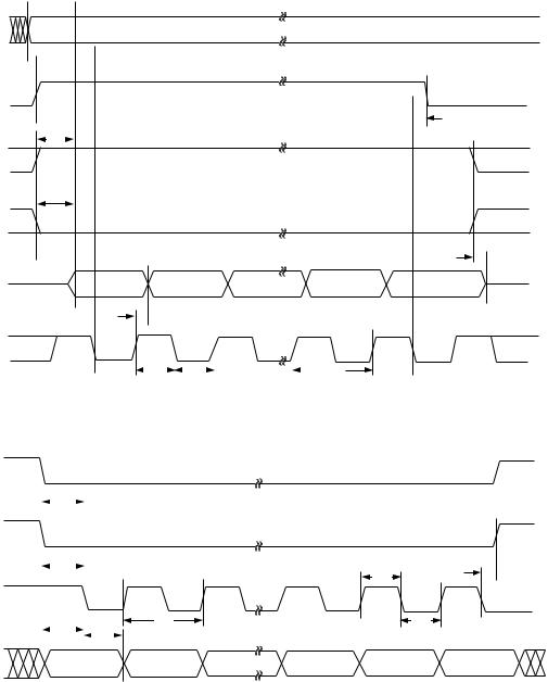
CLKIN
t2 |
|
|
t1 |
|
|
SYNC |
|
|
t3 |
t4 |
t5 |
|
||
|
|
|
MCLK |
|
|
(FS) |
|
|
MDATA |
DATA VALID |
DATA VALID |
|
t6 |
t7 |
|
|
|
t8 |
t9 |
|
TDATA |
VALID |
VALID |
Figure 3. AD1555/AD1556 Interface Timing |
||
t11 |
|
|
t10 |
|
|
RESET |
|
|
|
t2 |
|
|
t1 |
|
CLKIN |
|
|
SYNC |
|
|
|
t12 |
t13 |
|
t12 |
|
DRDY |
|
|
|
|
t14 |
ERROR |
|
|
Figure 4. AD1556 RESET, DRDY, and Overwrite Timings |
||
–6– |
REV. B |
 t15
t15 
RSEL
 t16
t16 
 t17
t17 
DRDY
 t18
t18 
t19
R/W
 t20
t20 
t21
CS
 t22
t22 
DOUT |
MSB |
SCLK
CS |
|
|
|
|
|
|
|
|
|
|
|
|
|
|
|
|
|
|
|
|
|
|
|
|
|
|
|
|
|
|
|
|
t29 |
|
|
|
|
|
|
|
|
|
|
|
|
|
|
|
|
|
|
|
|
|
|
|
|
|
|
R/W |
|
|
|
|
|
|
|
|
|
|
|
|
|
|
|
|
|
|
|
|
|
|
t30 |
|
|
|
|
|
|
|
|
|
|
|
|
|
|
|
|
SCLK |
|
|
|
|
|
|
|||
|
|
|
|
|
|
|
|
|
|
|
|
|
|
|
|
|
|
t32 |
|
|
|
|
t31 |
|
|
|
|||
|
|
|
|
|
|||||
|
|
|
|
|
|
|
|
||
DIN |
|
|
|
MSB |
|||||
|
|
|
|
|
|
|
|
|
|
t27 
MSB–1 |
LSB+1 |
LSB |
 t23
t23
|
|
|
|
|
|
|
|
|
|
|
|
|
|
|
|
|
|
|
|
|
|
|
|
|
t26 |
|
t24 |
|
|
|
|
t25 |
|
|
|
|
|
|
|
|
|
|
|
|
|
|
|
|
|
Figure 5. Serial Read Timing
|
t24 |
t26 |
t25 |
MSB–1 |
LSB+1 |
Figure 6. Serial Write Timing
AD1555/AD1556
 t28
t28
HI-Z
 t33
t33
LSB
REV. B |
–7– |

AD1555/AD1556
ABSOLUTE MAXIMUM RATINGS1 |
|
|
|
Analog Inputs |
|
|
|
Pins 7, 8, 23, 24, 25, 28 . . . . . . |
ÐVA Ð 0.3 V to +VA + 0.3 V |
||
AIN(+), AIN(Ð) DC Input Current . . . |
. . . . |
. . . . ±100 mA |
|
AIN(+), AIN(Ð) 2 s Pulse Input Current . . |
. . . . . . ±1.5 A |
||
Supply Voltages |
|
|
|
+VA to ÐVA . . . . . . . . . . . . . . . . . |
. . . . . |
. . . |
Ð0.3 V to +14 V |
+VA to AGND . . . . . . . . . . . . . . |
. . . . . . |
. . . |
Ð0.3 V to +7 V |
ÐVA to AGND . . . . . . . . . . . . . . |
. . . . . . |
. . . |
Ð7 V to +0.3 V |
VL to DGND . . . . . . . . . . . . . . . |
. . . . . . |
. . . |
Ð0.3 V to +7 V |
Ground Voltage Differences |
|
|
±0.3 V |
DGND, AGND1, AGND2, AGND3 . . |
. . . |
||
Digital Inputs . . . . . . . . . . . . . . . . |
. . . . |
Ð0.3 V to VL + 0.3 V |
|
Internal Power Dissipation2 |
|
|
|
AD1555 . . . . . . . . . . . . . . . . . . . |
. . . . . . |
. . . |
. . . . . . . 1.8 W |
AD1556 . . . . . . . . . . . . . . . . . . . |
. . . . . . |
. . . |
. . . . . . . 1.8 W |
Junction Temperature . . . . . . . . . . . . . . . . . |
. . . . . . . . 150°C |
Storage Temperature . . . . . . . . . . . . . . . . . . |
Ð65°C to +150°C |
Lead Temperature Range |
300°C |
(Soldering 10 sec) . . . . . . . . . . . . . . . . . . . |
NOTES
1Stresses above those listed under Absolute Maximum Ratings may cause permanent damage to the device. This is a stress rating only; functional operation of the device at these or any other conditions above those indicated in the operational section of this specification is not implied. Exposure to absolute maximum rating conditions for extended periods may affect device reliability.
2Specification is for device in free air:
28-lead PLCC: θJA = 36°C/W, θJC = 20°C/W
44-lead MQFP: θJA = 36°C/W, θJC = 14°C/W
ORDERING GUIDE
|
Temperature |
Package |
Package |
Model |
Range* |
Description |
Option |
|
|
|
|
AD1555AP |
0°C to 85°C |
Plastic Lead Chip Carrier |
P-28A |
AD1555APRL |
0°C to 85°C |
Plastic Lead Chip Carrier |
P-28A |
AD1555BP |
Ð55°C to +85 °C |
Plastic Lead Chip Carrier |
P-28A |
AD1555BPRL |
Ð55°C to +85 °C |
Plastic Lead Chip Carrier |
P-28A |
AD1556AS |
Ð55°C to +85 °C |
Plastic Quad Flatpack |
S-44A |
AD1556ASRL |
Ð55°C to +85 °C |
Plastic Quad Flatpack |
S-44A |
EVAL-AD1555/AD1556EB |
|
|
Evaluation Board |
AD1555/56-REF |
|
|
Reference Design |
|
|
|
|
*Contact factory for extended temperature range.
CAUTION
ESD (electrostatic discharge) sensitive device. Electrostatic charges as high as 4000 V readily accumulate on the human body and test equipment and can discharge without detection. Although the AD1555/AD1556 features proprietary ESD protection circuitry, permanent damage may occur on devices subjected to high energy electrostatic discharges. Therefore, proper ESD precautions are recommended to avoid performance degradation or loss of functionality.
WARNING!
ESD SENSITIVE DEVICE
–8– |
REV. B |
 Loading...