


White Electronic Designs WMS1M1-35DEMA, WMS1M1-35DEM, WMS1M1-35DEIA, WMS1M1-35DEI, WMS1M1-35DECA Datasheet
...
WMS1M1-XDEX
1Mx1 SRAM MONOLITHIC ADVANCED*
PIN CONFIGURATION
TOP VIEW
A10 |
|
|
1 |
32 |
|
VCC |
||||
|
|
|
||||||||
A11 |
|
|
2 |
31 |
|
NC |
||||
|
|
|
||||||||
A12 |
|
|
3 |
30 |
|
A9 |
||||
|
|
|
||||||||
|
NC |
|
|
4 |
29 |
|
A8 |
|||
|
|
|
||||||||
A13 |
|
|
5 |
28 |
|
A7 |
||||
|
|
|
||||||||
A14 |
|
|
6 |
27 |
|
A6 |
||||
|
|
|
||||||||
A15 |
|
|
7 |
26 |
|
A5 |
||||
|
|
|
||||||||
|
NC |
|
|
8 |
25 |
|
A4 |
|||
|
|
|
||||||||
A16 |
|
|
9 |
24 |
|
A3 |
||||
|
|
|
||||||||
A17 |
|
|
10 |
23 |
|
NC |
||||
|
|
|
||||||||
A18 |
|
|
11 |
22 |
|
A2 |
||||
|
|
|
||||||||
A19 |
|
|
12 |
21 |
|
NC |
||||
|
|
|
||||||||
|
NC |
|
|
13 |
20 |
|
A1 |
|||
|
|
|
||||||||
|
Q |
|
|
14 |
19 |
|
A0 |
|||
|
|
|
||||||||
|
|
|
15 |
18 |
|
D |
||||
|
WE |
|
|
|
||||||
|
|
|||||||||
GND |
|
16 |
17 |
|
|
|||||
|
|
|
CS |
|
||||||
|
|
|
|
|
|
|
|
|
|
|
PIN DESCRIPTION
A0-19 |
Address Inputs |
||||
D,Q |
Data Input, Data Output |
||||
|
|
|
|
|
|
|
|
|
|
Chip Select |
|
|
|
CS |
|||
|
|
|
|
|
|
|
WE |
Write Enable |
|||
|
|
|
|
|
|
VCC |
Power Supply |
||||
|
|
|
|
|
|
GND |
Ground |
||||
|
|
|
|
|
|
|
NC |
Not Connected |
|||
|
|
|
|
|
|
FEATURES
■Access Times 20, 25, 35ns
■MIL-STD-883 Compliant Devices Available
■Packaging
•32 lead, Ceramic SOJ (Package 101)
■Commercial, Industrial and Military Temperature Ranges
■Organized as 1M x 1
■5 Volt Power Supply
■Low Power CMOS
■TTL Compatible Inputs and Outputs
■2V Data Retention Devices also Available for Battery Back-Up Operation
*This data sheet describes a product that may or may not be under development and is subject to change or cancellation without notice.
2
MONOLITHICS SRAM
May 1997 |
1 |
White Microelectronics • Phoenix, AZ • (602) 437-1520 |
WMS1M1-XDEX
2
MONOLITHICS SRAM
ABSOLUTE MAXIMUM RATINGS
Parameter |
Symbol |
Min |
Max |
Unit |
Operating Temperature |
TA |
-55 |
+125 |
°C |
Storage Temperature |
TSTG |
-65 |
+150 |
°C |
Signal Voltage Relative to GND |
VG |
-0.5 |
Vcc+0.5 |
V |
Junction Temperature |
TJ |
|
150 |
°C |
Supply Voltage |
VCC |
-0.5 |
7.0 |
V |
|
|
|
|
|
RECOMMENDED OPERATING CONDITIONS
Parameter |
Symbol |
Min |
Max |
Unit |
|
|
|
|
|
Supply Voltage |
VCC |
4.5 |
5.5 |
V |
Input High Voltage |
VIH |
2.2 |
VCC + 0.3 |
V |
Input Low Voltage |
VIL |
-0.5 |
+0.8 |
V |
Operating Temp. (Mil.) |
TA |
-55 |
+125 |
°C |
TRUTH TABLE
|
|
|
|
|
|
|
|
|
|
CS |
|
WE |
|
Mode |
I/O Pin |
Cycle |
Current |
||
|
H |
|
X |
|
Not Selected |
High-Z |
— |
ISB1, ISB2 |
|
|
L |
|
H |
|
Read |
DOUT |
Read |
ICCA |
|
|
L |
|
L |
|
Write |
High-Z |
Write |
ICCA |
|
H = High, L = Low, X = Don't Care
CAPACITANCE
(TA = +25°C)
Parameter |
Symbol |
Condition |
Max |
Unit |
|
|
|
|
|
Input capacitance |
CIN |
VIN = 0V, f = 1.0MHz |
15 |
pF |
Output capicitance |
COUT |
VOUT = 0V, f = 1.0MHz |
15 |
pF |
|
|
|
|
|
This parameter is guaranteed by design but not tested.
DC CHARACTERISTICS
(VCC = 5.0V, GND = 0V, TA = -55°C to +125°C)
Parameter |
Sym |
|
|
|
|
|
Conditions |
Min |
Max |
Units |
|||||||
|
|
|
|
|
|
|
|
|
|
|
|
|
|
|
|
||
|
|
|
|
|
|
|
|
|
|
|
|
|
|
|
|
|
|
Input Leakage Current |
ILI |
|
VCC = 5.5, VIN = GND to VCC |
|
10 |
μA |
|
||||||||||
Output Leakage Current |
ILO |
|
|
|
|
|
= VIH, |
|
|
|
|
= VIH, VOUT = GND to VCC |
|
10 |
μA |
||
|
|
CS |
OE |
|
|||||||||||||
Operating Supply Current |
ICC |
|
|
|
= VIL, |
|
|
|
= VIH, f = 5MHz, Vcc = 5.5 |
|
105 |
mA |
|||||
|
CS |
OE |
|
||||||||||||||
Standby Current |
ISB |
|
|
= VIH, |
|
= VIH, f = 5MHz |
|
30 |
mA |
||||||||
|
CS |
OE |
|
||||||||||||||
Output Low Voltage |
VOL |
|
IOL = 8mA, VCC = 4.5 |
|
0.4 |
V |
|||||||||||
Output High Voltage |
VOH |
|
IOH = -4.0mA, VCC = 4.5 |
2.4 |
|
V |
|||||||||||
|
|
|
|
|
|
|
|
|
|
|
|
|
|
|
|
|
|
NOTE: DC test conditions: VIH = VCC -0.3V, VIL = 0.3V
|
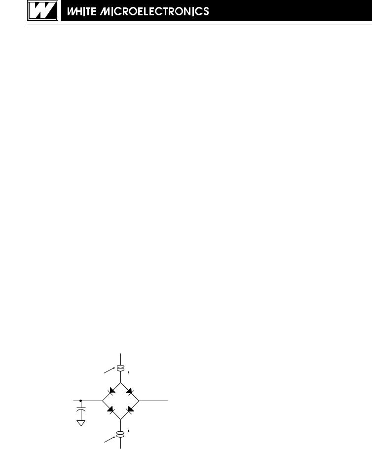
AC TEST CIRCUIT |
|
AC TEST CONDITIONS |
|
|
||
|
|
I OL |
|
|
|
|
|
|
|
|
Parameter |
Typ |
Unit |
|
|
|
Current Source |
|
|
Input Pulse Levels |
VIL = 0, VIH = 3.0 |
V |
|
|
|
|
|
|
|
|
|
|
|
|
|
Input Rise and Fall |
5 |
ns |
|
|
|
|
|
|
|
|
|
|
|
|
|
Input and Output Reference Level |
1.5 |
V |
|
|
|
VZ ≈1.5V |
|
|
|
|
|
|
D.U.T. |
Output Timing Reference Level |
1.5 |
V |
|
||
|
Ceff = 50 pf |
(Bipolar Supply) |
NOTES: |
|
|
|
|
|
|
|
|
|
|||
|
|
|
|
VZ is programmable from -2V to +7V. |
|
|
|
|
|
|
|
IOL & IOH programmable from 0 to 16mA. |
|
|
|
|
|
|
|
Tester Impedance Z0 = 75 Ω. |
|
|
|
|
|
IOH |
|
VZ is typically the midpoint of VOH and VOL. |
|
|
|
|
|
|
IOL & IOH are adjusted to simulate a typical resistive load circuit. |
||||
|
Current Source |
|
|
ATE tester includes jig capacitance. |
|
|
|
|
|
|
|
|
|
|
|
|
|
|
|
|
|
|
|
|
|
|
|
|
|
|
|
White Microelectronics • Phoenix, AZ • (602) 437-1520 |
2 |
|
|
|
|
||
 Loading...