


White Electronic Designs WS512K32N-45H1QA, WS512K32N-45H1Q, WS512K32N-45H1MA, WS512K32N-45H1IA, WS512K32N-45H1I Datasheet
...WS512K32-XXX
512Kx32 SRAM MODULE, SMD 5962-94611
FEATURES
νAccess Times of 15*, 17, 20, 25, 35, 45, 55ns
νPackaging
•66 pin, PGA Type, 1.075" square, Hermetic Ceramic HIP (Package 400).
•68 lead, 40mm Hermetic Low Profile CQFP, 3.5mm (0.140") (Package 502)1, Package to be developed.
•68 lead, Hermetic CQFP (G2T)1, 22.4mm (0.880") square (Package 509) 4.57mm (0.180") height.
Designed to fit JEDEC 68 lead 0.990" CQFJ footprint (Fig. 3).
•68 lead, Hermetic CQFP (G1U), 23.9mm (0.940") square (Package 519) 3.57mm (0.140") height.
Designed to fit JEDEC 68 lead 0.990" CQFJ footprint (Fig. 3).
•68 lead, Hermetic CQFP (G1U), 23.9mm (0.940") square (Package 524) 4.06mm (0.160") height.
νOrganized as 512Kx32, User Configurable as 1Mx16 or 2Mx8
νCommercial, Industrial and Military Temperature Ranges
νTTL Compatible Inputs and Outputs
ν5 Volt Power Supply
νLow Power CMOS
νBuilt-in Decoupling Caps and Multiple Ground Pins for Low Noise Operation
νWeight
WS512K32-XH1X - 13 grams typical WS512K32-XG2TX1 - 8 grams typical WS512K32-XG1UX - 5 grams typical WS512K32-XG1TX - 5 grams typical WS512K32-XG4TX1 - 20 grams typical
* 15ns Access Time available only in Commercial and Industrial Temperature. This speed is not fully characterized and is subject to change without notice.
Note 1: Package Not Recommended For New Design
FIG. 1 PIN CONFIGURATION FOR WS512K32N-XH1X |
|
|
TOP VIEW |
PIN DESCRIPTION |
|
|
I/O0-31 |
Data Inputs/Outputs |
|
A0-18 |
Address Inputs |
|
WE1-4 Write Enables |
|
|
CS1-4 |
Chip Selects |
|
OE |
Output Enable |
|
VCC |
Power Supply |
|
GND |
Ground |
|
NC |
Not Connected |
BLOCK DIAGRAM
November 2001 Rev. 9 |
1 |
White Electronic Designs Corporation • (602) 437-1520 • www.whiteedc.com |

WS512K32-XXX
FIG. 2 PIN CONFIGURATION FOR WS512K32-XG4TX1 |
|
|
|
|
|
|
|
|
|
|
|
|
|
|
|
|
|
|
|
|
|
|
|
|
|
|
|
|
|
|
|
|
|
|
|
||||||||||||||||||
|
|
|
|
|
|
TOP VIEW |
|
|
|
|
|
|
|
|
|
|
|
|
|
|
|
|
|
|
PIN DESCRIPTION |
||||||||||||||||||||||||||||
|
|
|
|
|
|
|
|
|
|
|
|
|
|
|
|
|
|
|
|
|
|
|
|
|
|
|
|
|
|
|
|
|
|
|
|
|
|
|
|
|
|
|
|
|
|||||||||
|
|
|
|
|
|
|
|
|
|
|
|
|
|
|
|
|
|
|
|
|
|
|
|
|
|
|
|
|
|
|
|
|
|
|
|
|
|
I/O0-31 |
Data Inputs/Outputs |
||||||||||||||
|
|
|
|
|
|
|
|
|
|
|
|
|
|
|
|
|
|
|
|
|
|
|
|
|
|
|
|
|
|
|
|
|
|
|
|
|
|
|
|
|
|
||||||||||||
|
|
|
|
|
|
|
|
|
|
|
|
|
|
|
|
|
|
|
|
|
|
|
|
|
|
|
|
|
|
|
|
|
|
|
|
|
|
A0-18 |
|
|
Address Inputs |
||||||||||||
|
|
|
|
|
|
|
|
|
|
|
|
|
|
|
|
|
|
|
|
|
|
|
|
|
|
|
|
|
|
|
|
|
|
|
|
|
|
|
WE |
|
|
|
|
Write Enables |
|||||||||
|
|
|
|
|
|
|
|
|
|
|
|
|
|
|
|
|
|
|
|
|
|
|
|
|
|
|
|
|
|
|
|
|
|
|
|
|
|
|
|
|
|
|
|
||||||||||
|
|
|
|
|
|
|
|
|
|
|
|
|
|
|
|
|
|
|
|
|
|
|
|
|
|
|
|
|
|
|
|
|
|
|
|
|
|
|
|
|
|
1-4 |
|
|
Chip Selects |
||||||||
|
|
|
|
|
|
|
|
|
|
|
|
|
|
|
|
|
|
|
|
|
|
|
|
|
|
|
|
|
|
|
|
|
|
|
|
|
|
CS |
|
|
|||||||||||||
|
|
|
|
|
|
|
|
|
|
|
|
|
|
|
|
|
|
|
|||||||||||||||||||||||||||||||||||
|
|
|
|
|
|
|
|
|
|
|
|
|
|
|
|
|
|
|
|
|
|
|
|
|
|
|
|
|
|
|
|
|
|
|
|
|
|
|
|
|
|
|
|
|
|
|
|
|
|
|
|
|
|
|
|
|
|
|
|
|
|
|
|
|
|
|
|
|
|
|
|
|
|
|
|
|
|
|
|
|
|
|
|
|
|
|
|
|
|
|
|
|
|
OE |
|
|
|
Output Enable |
|||||||||
|
|
|
|
|
|
|
|
|
|
|
|
|
|
|
|
|
|
|
|
|
|
|
|
|
|
|
|
|
|
|
|
|
|
|
|
|
|
|
|
|
|
|
|
|
|
|
|
|
|
|
|
|
|
|
|
|
|
|
|
|
|
|
|
|
|
|
|
|
|
|
|
|
|
|
|
|
|
|
|
|
|
|
|
|
|
|
|
|
|
|
|
|
VCC |
|
|
Power Supply |
|||||||||||
|
|
|
|
|
|
|
|
|
|
|
|
|
|
|
|
|
|
|
|
|
|
|
|
|
|
|
|
|
|
|
|
|
|
|
|
|
|
|
|
|
|||||||||||||
|
|
|
|
|
|
|
|
|
|
|
|
|
|
|
|
|
|
|
|
|
|
|
|
|
|
|
|
|
|
|
|
|
|
|
|
|
|
GND |
|
|
|
Ground |
|||||||||||
|
|
|
|
|
|
|
|
|
|
|
|
|
|
|
|
|
|
|
|||||||||||||||||||||||||||||||||||
|
|
|
|
|
|
|
|
|
|
|
|
|
|
|
|
|
|
|
|
|
|
|
|
|
|
|
|
|
|
|
|
|
|
|
|
|
|
|
NC |
|
|
Not Connected |
|||||||||||
|
|
|
|
|
|
|
|
|
|
|
|
|
|
|
|
|
|
|
|||||||||||||||||||||||||||||||||||
|
|
|
|
|
|
|
|
|
|
|
|
|
|
|
|
|
|
|
|
|
|
|
|
|
|
|
|
|
|
|
|
|
|
|
|
|
|
|
|
|
|
|
|
|
|
|
|
|
|
|
|
|
|
|
|
|
|
|
|
|
|
|
|
|
|
|
|
|
|
|
|
|
|
|
|
|
|
|
|
BLOCK DIAGRAM |
|
|
|
|
|
|
|
|
|
||||||||||||||||||
|
|
|
|
|
|
|
|
|
|
|
|
|
|
|
|
|
|
|
|
|
|
|
|
|
|
|
|
||||||||||||||||||||||||||
|
|
|
|
|
|
|
|
|
|
|
|
|
|
|
|
|
|
|
|
|
|
|
|
|
|
|
|
||||||||||||||||||||||||||
|
|
|
|
|
|
|
|
|
|
|
|
|
|
|
|
|
|
|
|
|
|
|
|
|
|
|
|
|
|
|
|
|
|
|
|
|
|
|
|
|
|
|
|
|
|
|
|
|
|
|
|
|
|
|
|
|
|
|
|
|
|
|
|
|
|
|
|
|
|
|
|
|
|
|
|
|
|
|
|
|
|
|
|
|
|
|
|
|
|
|
|
|
|
|
|
|
|
|
|
|
|
|
|
|
|
|
|
|
|
|
|
|
|
|
|
|
|
|
|
|
|
|
|
|
|
|
|
|
|
|
|
|
|
|
|
|
|
|
|
|
|
|
|
|
|
|
|
|
|
|
|
|
|
|
|
|
|
|
|
|
|
|
|
|
|
|
|
|
|
|
|
|
|
|
|
|
|
|
|
|
|
|
|
|
|
|
|
|
|
|
|
|
|
|
|
|
|
|
|
|
|
|
|
|
|
|
|
|
|
|
|
|
|
|
|
|
|
|
|
|
|
|
|
|
|
|
|
|
|
|
|
|
|
|
|
|
|
|
|
|
|
|
|
|
|
|
|
|
|
|
|
|
|
|
|
|
|
|
|
|
|
|
|
|
|
|
|
|
|
|
|
|
|
|
|
|
|
|
|
|
|
|
|
|
|
|
|
|
|
|
|
|
|
|
|
|
|
|
|
|
|
|
|
|
|
|
|
|
|
|
|
|
|
|
|
|
|
|
|
|
|
|
|
|
|
|
|
|
|
|
|
|
|
|
|
|
|
|
|
|
|
|
|
|
|
|
|
|
|
|
|
|
|
|
|
|
|
|
|
|
|
|
|
|
|
|
|
|
|
|
|
|
|
|
|
|
|
Note 1: Package Not Recommended For New Design
FIG. 3 PIN CONFIGURATION FOR WS512K32-XG2TX1, WS512K32-XG1TX
AND WS512K32-XG1UX
TOP VIEW
The White 68 lead CQFP fills the same fit and function as the JEDEC 68 lead CQFJ or 68 PLCC. But the CQFJ has the TCE and lead inspection advantage of the CQFP form.
PIN DESCRIPTION
|
I/O0-31 |
Data Inputs/Outputs |
|||||
|
|
|
|
||||
|
|
A0-18 |
Address Inputs |
||||
|
|
|
|
|
|
|
|
|
|
|
|
|
1-4 |
Write Enables |
|
|
WE |
||||||
|
|
|
|
|
|
||
|
|
|
|
1-4 |
Chip Selects |
||
|
|
CS |
|||||
|
|
|
|
|
|
||
|
|
|
|
|
|
|
Output Enable |
|
|
|
OE |
||||
|
|
|
|
||||
|
|
VCC |
Power Supply |
||||
|
|
|
|
||||
|
|
GND |
Ground |
||||
|
|
|
|
||||
|
|
NC |
Not Connected |
||||
|
|
|
|
|
|
|
|
BLOCK DIAGRAM
Note 1: Package Not Recommended For New Design
White Electronic Designs Corporation • (602) 437-1520 • www.whiteedc.com |
2 |

WS512K32-XXX
ABSOLUTE MAXIMUM RATINGS
Parameter |
Symbol |
Min |
Max |
Unit |
|
|
|
|
|
Operating Temperature |
TA |
-55 |
+125 |
°C |
|
|
|
|
|
Storage Temperature |
TSTG |
-65 |
+150 |
°C |
|
|
|
|
|
Signal Voltage Relative to GND |
VG |
-0.5 |
Vcc+0.5 |
V |
|
|
|
|
|
Junction Temperature |
TJ |
|
150 |
°C |
|
|
|
|
|
Supply Voltage |
VCC |
-0.5 |
7.0 |
V |
|
|
|
|
|
RECOMMENDED OPERATING CONDITIONS
Parameter |
Symbol |
Min |
Max |
Unit |
|
|
|
|
|
Supply Voltage |
VCC |
4.5 |
5.5 |
V |
|
|
|
|
|
Input High Voltage |
VIH |
2.2 |
VCC + 0.3 |
V |
|
|
|
|
|
Input Low Voltage |
VIL |
-0.5 |
+0.8 |
V |
|
|
|
|
|
Operating Temp (Mil) |
TA |
-55 |
+125 |
°C |
|
|
|
|
|
TRUTH TABLE
|
|
|
|
|
|
|
|
|
Mode |
Data I/O |
Power |
||
|
CS |
|
|
OE |
|
|
WE |
||||||
|
|
|
|
|
|
|
|
|
|
|
|
||
|
H |
|
X |
|
|
X |
|
Standby |
High Z |
Standby |
|
||
|
|
|
|
|
|
|
|
|
|
|
|
||
|
L |
|
L |
|
|
H |
|
Read |
Data Out |
Active |
|||
|
|
|
|
|
|
|
|
|
|
|
|
||
|
L |
|
H |
|
|
H |
|
Out Disable |
High Z |
Active |
|
||
|
|
|
|
|
|
|
|
|
|
|
|
|
|
|
L |
|
X |
|
|
L |
|
W r i t e |
Data In |
Active |
|||
CAPACITANCE
(TA = +25°C)
|
Parameter |
Symbol |
Conditions |
Max |
Unit |
||||
|
|
|
|
|
capacitance |
COE |
VIN = 0 V, f = 1.0 MHz |
50 |
pF |
|
OE |
|
|||||||
|
|
|
|
|
1-4 capacitance |
CWE |
VIN = 0 V, f = 1.0 MHz |
|
pF |
|
WE |
|
|||||||
|
|
|
|
|
HIP (PGA) |
|
|
2 0 |
|
|
|
|
|
|
CQFP G4T |
|
|
5 0 |
|
|
|
|
|
|
CQFPG2T/G1U/G1T |
|
|
20 |
|
|
|
CCS |
VIN = 0 V, f = 1.0 MHz |
20 |
pF |
||||
|
|
CS |
1-4 capacitance |
||||||
|
Data I/O capacitance |
CI/O |
VI/O = 0 V, f = 1.0 MHz |
20 |
pF |
||||
|
|
|
|
|
|
|
|
||
|
Addressinputcapacitance |
CAD |
VIN = 0 V, f = 1.0 MHz |
50 |
pF |
||||
|
|
|
|
|
|
|
|
|
|
This parameter is guaranteed by design but not tested.
DC CHARACTERISTICS
(VCC = 5.0V, VSS = 0V, TA = -55°C to +125°C)
Parameter |
|
Symbol |
|
|
|
|
|
|
|
|
|
|
|
Conditions |
|
|
Units |
||
|
|
|
|
|
|
|
|
|
|
|
|
|
|
|
|
|
Min |
Max |
|
Input Leakage Current |
ILI |
VCC = 5.5, VIN = GND to VCC |
|
|
1 0 |
µA |
|||||||||||||
Output Leakage Current |
ILO |
|
|
|
|
|
|
= VIH, |
|
|
= VIH, VOUT = GND to VCC |
|
1 0 |
µA |
|||||
CS |
OE |
|
|||||||||||||||||
Operating Supply Current x 32 Mode |
ICC x 32 |
|
|
|
|
= VIL, |
|
|
|
|
= VIH, f = 5MHz, Vcc = 5.5 |
|
660 |
m A |
|||||
|
CS |
OE |
|
||||||||||||||||
Standby Current |
ISB |
|
|
= VIH, |
|
= VIH, f = 5MHz, Vcc = 5.5 |
|
8 0 |
m A |
||||||||||
|
CS |
OE |
|
||||||||||||||||
Output |
Low |
Voltage |
VOL |
IOL = 8mA for 15 - 35ns, |
|
|
0.4 |
V |
|||||||||||
|
|
|
|
IOL = 2.1mA for 45 - 55ns, Vcc = 4.5 |
|
|
|
||||||||||||
Output |
High |
Voltage |
VOH |
IOH = -4.0mA for 15 - 35ns, |
|
2.4 |
|
V |
|||||||||||
|
|
|
|
IOH = -1.0mA for 45 - 55ns, |
Vcc = 4.5 |
|
|
|
|||||||||||
|
|
|
|
|
|
|
|
|
|
|
|
|
|
|
|
|
|
|
|
NOTE: DC test conditions: VIH = VCC -0.3V, VIL = 0.3V
DATA RETENTION CHARACTERISTICS
(TA = -55°C to +125°C)
Parameter |
Symbol |
|
Conditions |
|
|
Units |
|
|
|
|
|
|
Min |
Max |
|
Data Retention Supply Voltage |
VDR |
|
|
£ VCC -0.2V |
2.0 |
5.5 |
V |
|
CS |
||||||
Data Retention Current |
ICCDR1 |
|
|
VCC = 3V |
|
28 |
mA |
Low Power Data Retention |
ICCDR2 |
|
|
VCC = 3V |
|
16 |
mA |
Current (WS512K32L-XXX) |
|
|
|
|
|
|
|
3 |
White Electronic Designs Corporation • (602) 437-1520 • www.whiteedc.com |
WS512K32-XXX
AC CHARACTERISTICS
(VCC = 5.0V, VSS = 0V, TA = -55°C to +125°C)
Parameter |
Symbol |
- 1 5 * |
-17 |
-20 |
-25 |
|
-35 |
-45 |
-55 |
Units |
|||||||
Read Cycle |
|
Min Max |
Min Max |
Min Max |
Min Max |
Min |
|
Max |
Min Max |
Min Max |
|
||||||
Read Cycle Time |
tRC |
1 5 |
|
1 7 |
|
2 0 |
|
2 5 |
|
3 5 |
|
|
4 5 |
|
5 5 |
|
n s |
|
|
|
|
|
|
|
|
|
|
|
|
|
|
|
|
|
|
Address Access Time |
tAA |
|
1 5 |
|
1 7 |
|
2 0 |
|
2 5 |
|
|
3 5 |
|
4 5 |
|
5 5 |
n s |
Output Hold from Address Change |
tOH |
0 |
|
0 |
|
0 |
|
0 |
|
0 |
|
|
0 |
|
0 |
|
n s |
Chip Select Access Time |
tACS |
|
1 5 |
|
1 7 |
|
2 0 |
|
2 5 |
|
|
3 5 |
|
4 5 |
|
5 5 |
n s |
|
|
|
|
|
|
|
|
|
|
|
|
|
|
|
|
|
|
Output Enable to Output Valid |
tOE |
|
8 |
|
9 |
|
1 0 |
|
1 2 |
|
|
2 5 |
|
2 5 |
|
2 5 |
n s |
|
|
|
|
|
|
|
|
|
|
|
|
|
|
|
|
|
|
Chip Select to Output in Low Z |
tCLZ1 |
2 |
|
2 |
|
2 |
|
2 |
|
4 |
|
|
4 |
|
4 |
|
n s |
Output Enable to Output in Low Z |
tOLZ1 |
0 |
|
0 |
|
0 |
|
0 |
|
0 |
|
|
0 |
|
0 |
|
n s |
Chip Disable to Output in High Z |
tCHZ1 |
|
1 2 |
|
1 2 |
|
1 2 |
|
1 2 |
|
|
1 5 |
|
2 0 |
|
2 0 |
n s |
Output Disable to Output in High Z |
tOHZ1 |
|
1 2 |
|
1 2 |
|
1 2 |
|
1 2 |
|
|
1 5 |
|
2 0 |
|
2 0 |
n s |
* 15ns Access Time available only in Commercial and Industrial Temperature. This speed is not fully characterized and is subject to change without notice. 1. This parameter is guaranteed by design but not tested.
AC CHARACTERISTICS
(VCC = 5.0V, VSS = 0V, TA = -55°C to +125°C)
Parameter |
|
Symbol |
-15* |
-17 |
-20 |
-25 |
-35 |
-45 |
-55 |
Units |
||||||||
Write Cycle |
|
|
Min Max |
Min Max |
Min Max |
Min Max |
Min Max |
Min Max |
Min Max |
|
||||||||
|
|
|
|
|
|
|
|
|
|
|
|
|
|
|
|
|
||
Write Cycle Time |
t WC |
1 5 |
|
1 7 |
|
2 0 |
|
2 5 |
|
3 5 |
|
4 5 |
|
5 5 |
|
n s |
||
Chip Select to End of Write |
t CW |
1 3 |
|
1 5 |
|
1 5 |
|
1 7 |
|
2 5 |
|
3 5 |
|
5 0 |
|
n s |
||
Address Valid to End of Write |
t AW |
1 3 |
|
1 5 |
|
1 5 |
|
1 7 |
|
2 5 |
|
3 5 |
|
5 0 |
|
n s |
||
Data Valid to End of Write |
t DW |
1 0 |
|
1 1 |
|
1 2 |
|
1 3 |
|
2 0 |
|
2 5 |
|
2 5 |
|
n s |
||
|
|
|
|
|
|
|
|
|
|
|
|
|
|
|
|
|
||
Write Pulse Width |
t WP |
1 3 |
|
1 5 |
|
1 5 |
|
1 7 |
|
2 5 |
|
3 5 |
|
4 0 |
|
n s |
||
Address |
Setup |
Time |
t AS |
2 |
|
2 |
|
2 |
|
2 |
|
2 |
|
2 |
|
2 |
|
n s |
Address |
Hold |
Time |
t AH |
0 |
|
0 |
|
0 |
|
0 |
|
0 |
|
5 |
|
5 |
|
n s |
|
|
|
|
|
|
|
|
|
|
|
|
|
|
|
|
|
||
Output Active from End of Write |
t OW1 |
2 |
|
2 |
|
3 |
|
4 |
|
4 |
|
5 |
|
5 |
|
n s |
||
Write Enable to Output in High Z |
t WHZ 1 |
|
8 |
|
9 |
|
1 1 |
|
1 3 |
|
1 5 |
|
2 0 |
|
2 0 |
n s |
||
Data Hold Time |
t DH |
0 |
|
0 |
|
0 |
|
0 |
|
0 |
|
0 |
|
0 |
|
n s |
||
|
|
|
|
|
|
|
|
|
|
|
|
|
|
|
|
|
|
|
* |
15ns Access Time available only in Commercial and Industrial Temperature. This speed is not fully characterized and is subject to change without notice. |
|
1. |
This parameter is guaranteed by design but |
not tested. |
2 . |
The Address Setup Time of minimum 2ns is |
for the G2T, G1U and H1 packages. tAS minimum for the G4T package is 0ns. |
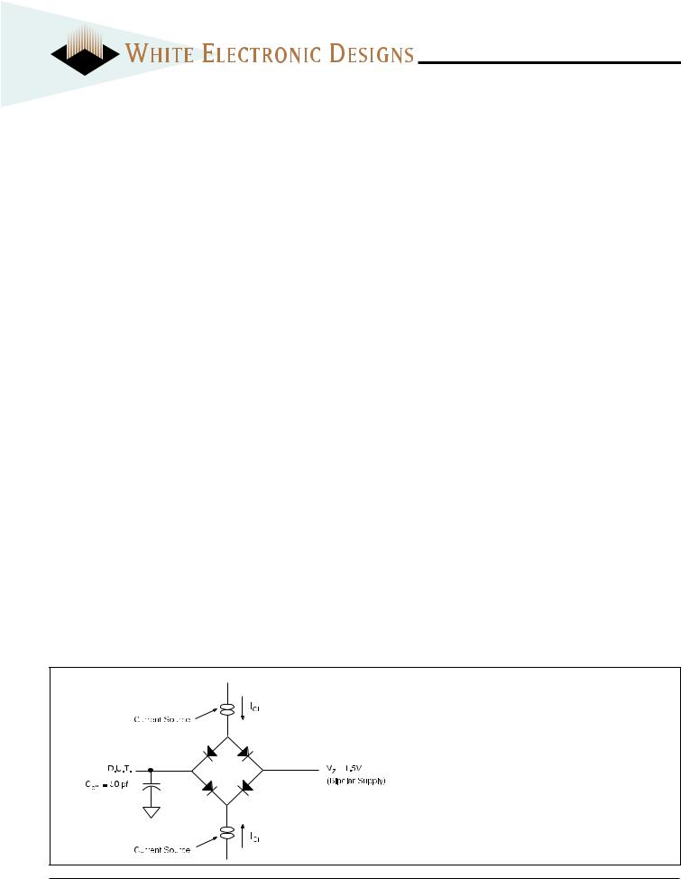
FIG. 4
AC TEST CIRCUIT
AC TEST CONDITIONS
Parameter |
|
Typ |
Unit |
|
|
|
|
|
|
Input |
Pulse Levels |
VIL = 0, VIH = 3.0 |
V |
|
|
|
|
|
|
Input |
Rise and |
Fall |
5 |
n s |
|
|
|
||
Input and Output Reference Level |
1 . 5 |
V |
||
|
|
|
|
|
Output Timing |
Reference Level |
1 . 5 |
V |
|
|
|
|
|
|
N O T E S :
VZ is programmable from -2V to +7V. IOL & IOH programmable from 0 to 16mA. Tester Impedance Z0 = 75 ý.
VZ is typically the midpoint of VOH and VOL.
IOL & IOH are adjusted to simulate a typical resistive load circuit. ATE tester includes jig capacitance.
White Electronic Designs Corporation • (602) 437-1520 • www.whiteedc.com |
4 |
 Loading...