


WF128K64-120G4WC5
White Electronic Designs WF128K64-120G4WC5, WF128K64-60G4WM5, WF128K64-60G4WI5, WF128K64-60G4WC5, WF128K64-50G4WM5 Datasheet
...
White Microelectronics • Phoenix, AZ • (602) 437-1520
7
FLASH MODULES
1
128Kx64 5V FLASH MODULE
PRELIMINARY*
FEATURES
■ Access Times of 60, 70, 90, 120, 150ns
■ Packaging
•116 lead, 40mm square, Hermetic CQFP (Package 504)
■ Sector Architecture
•8 equal size sectors of 16KBytes each
•Any combination of sectors can be concurrently erased.
Also supports full chip erase
■ 100,000 Erase/Program Cycles Minimum (0°C to 70°C)
■ Data Retention, 10 Year Minimum at 125°C
■ Organized as 128Kx64, user configurable as 256Kx32,
512Kx16 or 1Mx8.
WF128K64-XG4WX5
■ Commercial, Industrial and Military Temperature Ranges
■ 5 Volt Programming; 5V ( ±10%) Supply
■ Low Power CMOS, 8mA Standby Typical
■ Hardware and Software Write Protection
■ TTL Compatible Inputs and Outputs
■ Built-in Decoupling Caps and Multiple Ground Pins for Low
Noise Operation
■ Weight
WF128K64-XG4WX5 - 20 grams typical
* This data sheet describes a product under development and is subject
to change without notice.
Note: Programming information available upon request.
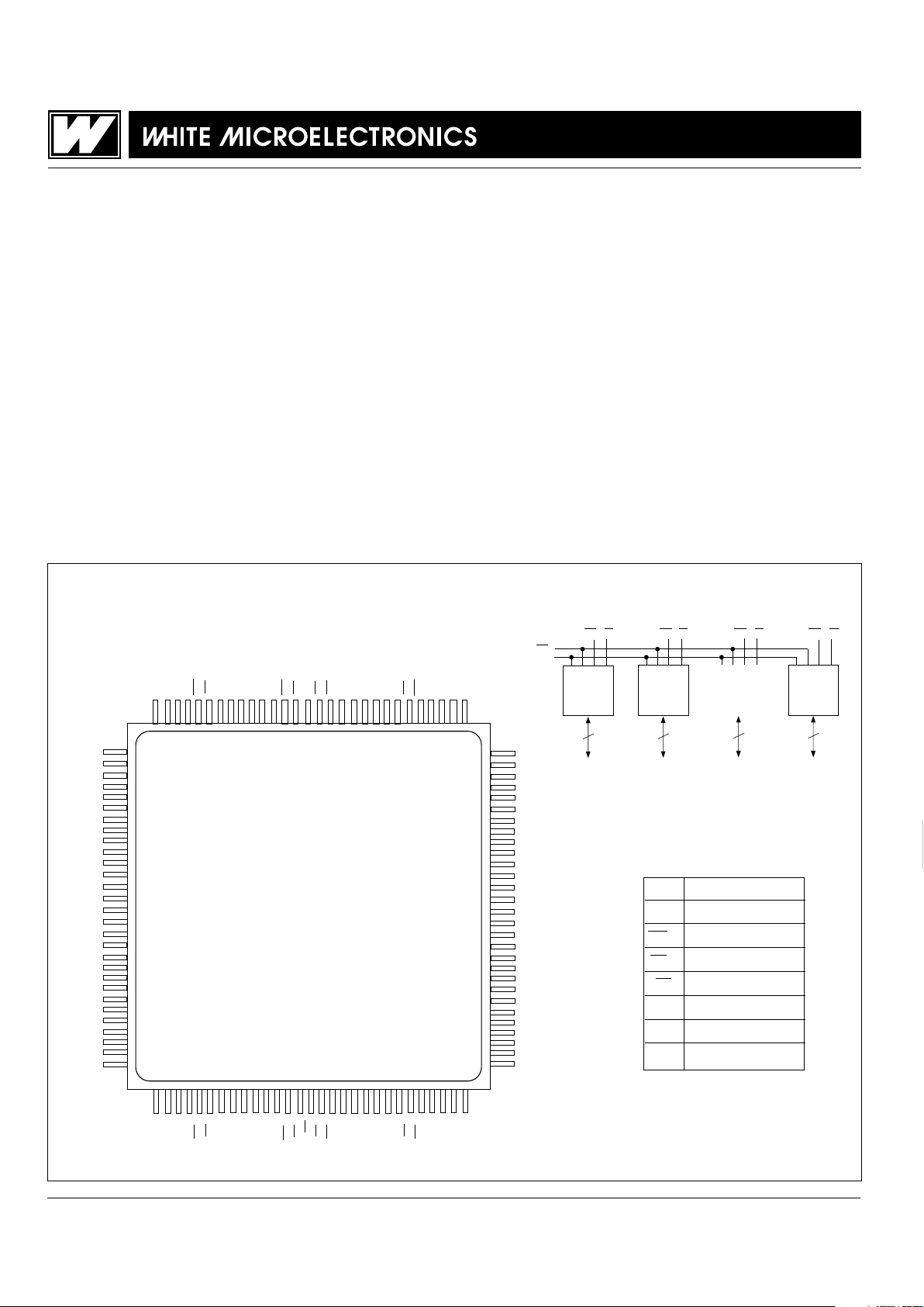
FIG. 1 PIN CONFIGURATION FOR WF128K64-XG4WX5
1
128K x 8
8
I/O
0-7
CS
1
2
128K x 8
8
I/O
8-15
CS
2
8
I/O...
CS
x
8
128K x 8
8
I/O
56-63
CS
8
A
0-16
OE
WE
1
WE
2
WE
x
WE
8
......
BLOCK DIAGRAM
16
17
18
19
20
21
22
23
24
25
26
27
28
29
30
31
32
33
34
35
36
37
38
39
40
41
42
43
44
1514131211
10
987654321
116
115
114
113
112
111
110
109
108
107
106
105
104
103
I/O
3
I/O
4
I/O
5
I/O
6
I/O
7
GND
I/O
8
I/O
9
I/O
10
I/O
11
I/O
12
I/O
13
I/O
14
I/O
15
GND
I/O
16
I/O
17
I/O
18
I/O
19
I/O
20
I/O
21
I/O
22
I/O
23
GND
I/O
24
I/O
25
I/O
26
I/O
27
I/O
28
I/O29I/O30I/O
31
V
CC
WE
3
CS
3
NCNCNC
NC
A
16A15
WE
4
CS
4
OE
CS
5WE5
A14A13A12A11A
10
NC
CS
6
WE
6
V
CC
I/O32I/O33I/O
34
I/O
60
I/O
59
I/O
58
I/O
57
I/O
56
GND
I/O
55
I/O
54
I/O
53
I/O
52
I/O
51
I/O
50
I/O
49
I/O
48
GND
I/O
47
I/O
46
I/O
45
I/O
44
I/O
43
I/O
42
I/O
41
I/O
40
GND
I/O
39
I/O
38
I/O
37
I/O
36
I/O
35
I/O2I/O1I/O0VCCWE2CS2NC
A0A1A2A3A4WE1CS1NC
CS8WE8A5A6A7A8A9NC
CS7WE7VCCI/O63I/O62I/O
61
4546474849505152535455565758596061626364656667686970717273
102
101
100
99
98
97
96
95
94
93
92
91
90
89
88
87
86
85
84
83
82
81
80
79
78
77
76
75
74
TOP VIEW
I/O0-63 Data Inputs/Outputs
A0-16 Address Inputs
WE1-8 Write Enables
CS1-8 Chip Selects
OE Output Enable
VCC Power Supply
GND Ground
NC Not Connected
PIN DESCRIPTION
September 1998
2
White Microelectronics • Phoenix, AZ • (602) 437-1520
7
FLASH MODULES
WF128K64-XG4WX5
ABSOLUTE MAXIMUM RATINGS (1)
NOTES:
1. Stresses above the absolute maximum rating may cause permanent damage
to the device. Extended operation at the maximum levels may degrade
performance and affect reliability.
2. Minimum DC voltage on input or I/O pins is -0.5V. During voltage transitions,
inputs may overshoot V
SS to -2.0 V for periods of up to 20ns. Maximum DC
voltage on output and I/O pins is V
CC + 0.5V. During voltage transitions,
outputs may overshoot to Vcc + 2.0 V for periods of up to 20ns.
3. Minimum DC input voltage on A
9 pin is -0.5V. During voltage transitions, A9 may
overshoot Vss to -2V for periods of up to 20ns. Maximum DC input voltage on A
9
is +13.5V which may overshoot to 14.0 V for periods up to 20ns.
DC CHARACTERISTICS - CMOS COMPATIBLE
(V
CC = 5.0V, VSS = 0V, TA = -55°C to +125°C)
NOTES:
1. The I
CC current listed includes both the DC operating current and the frequency dependent component (at 5 MHz).
The frequency component typically is less than 2 mA/MHz, with OE at V
IH.
2. I
CC active while Embedded Algorithm (program or erase) is in progress.
3. DC test conditions: V
IL = 0.3V, VIH = VCC - 0.3V
RECOMMENDED OPERATING CONDITIONS
Parameter Symbol Min Max Unit
Supply Voltage V
CC 4.5 5.5 V
Input High Voltage V
IH 2.0 VCC + 0.3 V
Input Low Voltage V
IL -0.5 +0.8 V
Operating Temp. (Mil.) T
A -55 +125 °C
A
9 Voltage for Sector Protect VID 11.5 12.5 V
Parameter Unit
Operating Temperature -55 to +125 °C
Supply Voltage Range (VCC) -2.0 to +7.0 V
Signal voltage range (any pin except A9) (2) -2.0 to +7.0 V
Storage Temperature Range -65 to +150 °C
Lead Temperature (soldering, 10 seconds) +300 °C
Data Retention Mil Temp 10 years
Endurance (write/erase cycles) Mil Temp 10,000 cycles min.
A
9 Voltage for sector protect (VID) (3) -2.0 to +14.0 V
CAPACITANCE
(T
A = +25°C)
Parameter
Symbol
Conditions Max Unit
OE capacitance COE
VIN = 0 V, f = 1.0 MHz
100 pF
WE capacitance CWE
VIN = 0 V, f = 1.0 MHz
20 pF
CS capacitance CCS
VIN = 0 V, f = 1.0 MHz
20 pF
Data I/O capacitance CI/O
V
I/O
= 0 V, f = 1.0 MHz
20 pF
Address input capacitance C
AD
V
IN
= 0 V, f = 1.0 MHz
100 pF
This parameter is guaranteed by design but not tested.
Parameter Symbol Conditions Min Max Unit
Input Leakage Current ILI VCC = 5.5, VIN = GND to VCC 10 µA
Output Leakage Current ILOx32 VCC = 5.5, VIN = GND to VCC 10 µA
VCC Active Current for Read (1) ICC1 CS = VIL, OE = VIH 280 mA
VCC Active Current for Program or Erase (2) ICC2 CS = VIL, OE = VIH 400 mA
VCC Standby Current ICC3 VCC = 5.5, CS = VIH, f = 5MHz 13 mA
VCC Static Current ICC4 VCC = 5.5, CS = VIH 1.2 mA
Output Low Voltage VOL IOL = 12.0 mA, VCC = 4.5 0.45 V
Output High Voltage V
OH1 IOH = -2.5 mA, VCC = 4.5 0.85 x V
VCC
Output High Voltage VOH2 IOH = -100 µA, VCC = 4.5 VCC V
-0.4
Low V
CC Lock Out Voltage VLKO 3.2 V

White Microelectronics • Phoenix, AZ • (602) 437-1520
7
FLASH MODULES
3
WF128K64-XG4WX5
AC CHARACTERISTICS – WRITE/ERASE/PROGRAM OPERATIONS, WE CONTROLLED
(V
CC = 5.0V, VSS = 0V, TA = -55°C to +125°C)
Parameter Symbol -60 -70 -90 -120 -150 Unit
Min Max Min Max Min Max Min Max Min Max
Write Cycle Time tAVAV tWC 60 70 90 120 150 ns
Chip Select Setup Time tELWL tCS 000 00ns
Write Enable Pulse Width tWLWH tWP 30 35 45 50 50 ns
Address Setup Time tAVWL tAS 000 00ns
Data Setup Time tDVWH tDS 30 30 45 50 50 ns
Data Hold Time tWHDX tDH 000 00ns
Address Hold Time tWLAX tAH 45 45 45 50 50 ns
Chip Select Hold Time tWHEH tCH 000 00ns
Write Enable Pulse Width High tWHWL tWPH 20 20 20 20 20 ns
Duration of Byte Programming Operation (min) tWHWH1 14 14 14 14 14 µs
Chip and Sector Erase Time tWHWH2 2.2 60 2.2 60 2.2 60 2.2 60 2.2 60 sec
Read Recovery Time Before Write tGHWL 000 00ns
VCC Setup Time tVCS 50 50 50 50 50 µs
Chip Programming Time 12.5 12.5 12.5 12.5 12.5 sec
Output Enable Setup Time tOES 0000 0ns
Output Enable Hold Time (1) t
OEH 10 10 10 10 10 ns
1. For Toggle and Data Polling.
AC CHARACTERISTICS – READ ONLY OPERATIONS
(VCC = 5.0V, VSS = 0V, TA = -55°C to +125°C)
Parameter Symbol -60 -70 -90 -120 -150 Unit
Min Max Min Max Min Max Min Max Min Max
Read Cycle Time tAVAV tRC 60 70 90 120 150 ns
Address Access Time tAVQV tACC 60 70 90 120 150 ns
Chip Select Access Time tELQV tCE 60 70 90 120 150 ns
OE to Output Valid tGLQV tOE 30 35 40 50 55 ns
Chip Select to Output High Z (1) tEHQZ tDF 20 20 25 30 35 ns
OE High to Output High Z (1) tGHQZ tDF 20 20 25 30 35 ns
Output Hold from Address, CS or OE Change, t
AXQX tOH 00000ns
whichever is first
1. Guaranteed by design, not tested.
 Loading...