


White Electronic Designs WSF512K16-39G2MA, WSF512K16-39G2M, WSF512K16-39G2I, WSF512K16-39G2IA, WSF512K16-39G2CA Datasheet
...WSF512K16-XXX
HI-RELIABILITY PRODUCT
512KX16 SRAM/FLASH MODULE, SMD 5962-96901
FEATURES
■Access Times of 35ns (SRAM) and 90ns (FLASH)
■Access Times of 70ns (SRAM) and 120ns (FLASH)
■Packaging
•66 pin, PGA Type, 1.385" square HIP, Hermetic Ceramic HIP (Package 402)
•68 lead, Hermetic CQFP (G2), 22mm (0.880") square (Package 500). Designed to fit JEDEC 68 lead 0.990” CQFJ footprint (Fig. 2)
■512Kx16 SRAM
■512Kx16 5V FLASH
■Organized as 512Kx16 of SRAM and 512Kx16 of Flash Memory with separate Data Busses
■Both blocks of memory are User Configurable as 1Mx8
■Low Power CMOS
■Commercial, Industrial and Military Temperature Ranges
■TTL Compatible Inputs and Outputs
■Built-in Decoupling Caps and Multiple Ground Pins for Low Noise Operation
■Weight - 13 grams typical
FLASH MEMORY FEATURES
■100,000 Erase/Program Cycles
■Sector Architecture
•8 equal size sectors of 64K bytes each
•Any combination of sectors can be concurrently erased. Also supports full chip erase
■5 Volt Programming; 5V ± 10% Supply
■Embedded Erase and Program Algorithms
■Hardware Write Protection
■Page Program Operation and Internal Program Control Time.
Note: Programming information available upon request.
FIG. 1 |
PIN CONFIGURATION FOR WSF512K16-XH2X |
|
|
|
|
|
|
|
|
|
|
|
|
|
|
|
|
|
|
|
|
|
|
PIN DESCRIPTION |
|||||||||||||||||||||||||||||||
|
|
|
TOP VIEW |
|
|
|
|
|
|
|
|
|
|
|
|
|
|
|
|
|
|
|
|
|
|
|
|
|
|
|
|
|
|
|
|
|
|
|
|
|
|
|
|
|
|
|
|
|
|||||||
|
|
|
|
|
|
|
|
|
|
|
|
|
|
|
|
|
|
|
|
|
|
|
|
|
|
|
|
|
|
|
|
|
|
|
|
|
|
|
FD0-15 |
|
Flash Data Inputs/Outputs |
|
|||||||||||||
1 |
12 |
23 |
|
34 |
45 |
|
56 |
|
|
|
|
|
|
|
|
|
|
|
|
|
|
|
|
|
|
|
|
|
|
|
|
|
|
|
|
|
|
|
|
|
|
|
|
|
|
|
|
|
|
|
|
|
|
|
|
|
|
|
|
|
|
|
|
|
|
|
|
|
|
|
|
|
|
|
|
|
|
|
|
|
|
|
|
|
|
|
|
SD0-15 |
SRAM Data Inputs/Outputs |
|
|||||||||||||||||||||
|
|
|
|
|
|
|
|
|
|
|
|
|
|
|
|
|
|
|
|
|
|
|
|
|
|
|
|
|
|
|
|
|
|
|
|
|
|
|
|
|
|||||||||||||||
|
SD8 |
SWE2 |
SD15 |
FD8 |
|
VCC |
FD15 |
|
|
|
|
|
|
|
|
|
|
|
|
|
|
|
|
|
|
|
|
|
|
|
|
|
|
|
|
|
|
|
|
|
|||||||||||||||
|
|
|
|
|
|
|
|
|
|
|
|
|
|
|
|
|
|
|
|
|
|
|
|
|
|
|
|
|
|
|
|
|
|
|
|
A0-18 |
|
|
|
|
|
Address Inputs |
|
||||||||||||
|
|
|
|
|
|
|
|
|
|
|
|
|
|
|
|
|
|
|
|
|
|
|
|
|
|
|
|
|
|
|
|
|
|
|
|
|
|
|
|
|
|
|
|
|
|
|
|
||||||||
|
SD9 |
SCS2 |
SD14 |
FD9 |
|
FCS2 |
FD14 |
|
|
|
|
|
|
|
|
|
|
|
|
|
|
|
|
|
|
|
|
|
|
|
|
|
|
|
|
|
|
|
|
|
|
|
1-2 |
|
|
|
SRAM Write Enable |
|
|||||||
|
|
|
|
|
|
|
|
|
|
|
|
|
|
|
|
|
|
|
|
|
|
|
|
|
|
|
|
|
|
|
|
|
SWE |
|
|
|
|
||||||||||||||||||
|
|
|
|
|
|
|
|
|
|
|
|
|
|
|
|
|
|
|
|
|
|
|
|
|
|
|
|
|
|
|
|
|
|
|
|
|
|
|
|
|
|
|
1-2 |
|
|
|
SRAM Chip Selects |
|
|||||||
|
SD10 |
GND |
SD13 |
FD10 |
|
FWE2 |
FD13 |
|
|
|
|
|
|
|
|
|
|
|
|
|
|
|
|
|
|
|
|
|
|
|
|
|
|
|
|
|
|
|
SCS |
|
|
|
|
||||||||||||
|
|
|
|
|
|
|
|
|
|
|
|
|
|
|
|
|
|
|
|
|
|
|
|
|
|
|
|
|
|
|
|
|
|
|
|
|
|
|
|
|
|
|
|
|
|
|
|
|
|
Output Enable |
|
||||
|
A13 |
SD11 |
SD12 |
A6 |
|
FD11 |
FD12 |
|
|
|
|
|
|
|
|
|
|
|
|
|
|
|
|
|
|
|
|
|
|
|
|
|
|
|
|
|
|
|
|
|
|
|
OE |
|
|
|
|
|
|
|
|||||
|
|
|
|
|
|
|
|
|
|
|
|
|
|
|
|
|
|
|
|
|
|
|
|
|
|
|
|
|
|
|
|
|
|
|
|
VCC |
|
|
|
|
|
Power Supply |
|
||||||||||||
|
|
|
|
|
|
|
|
|
|
|
|
|
|
|
|
|
|
|
|
|
|
|
|
|
|
|
|
|
|
|
|
|
|
|
|
|
|
|
|
|
|
|
|
|
|
|
|
||||||||
|
A14 |
A10 |
OE |
A7 |
|
A3 |
A0 |
|
|
|
|
|
|
|
|
|
|
|
|
|
|
|
|
|
|
|
|
|
|
|
|
|
|
|
|
|
|
|
|
|
|
GND |
|
|
|
|
|
Ground |
|
||||||
|
|
|
|
|
|
|
|
|
|
|
|
|
|
|
|
|
|
|
|
|
|
|
|
|
|
|
|
|
|
|
|
|
|
|
|
|
|
|
|
|
|
|
|
|
|
|
|
||||||||
|
A15 |
A11 |
A17 |
NC |
|
A4 |
A1 |
|
|
|
|
|
|
|
|
|
|
|
|
|
|
|
|
|
|
|
|
|
|
|
|
|
|
|
|
|
|
|
|
|
|
NC |
|
|
|
|
|
Not Connected |
|
||||||
|
|
|
|
|
|
|
|
|
|
|
|
|
|
|
|
|
|
|
|
|
|
|
|
|
|
|
|
|
|
|
|
|
|
|
|
|
|
|
|
1-2 |
|
|
|
Flash Write Enable |
|
||||||||||
|
A16 |
A12 |
SWE1 |
A8 |
|
A5 |
A2 |
|
|
|
|
|
|
|
|
|
|
|
|
|
|
|
|
|
|
|
|
|
|
|
|
|
|
|
|
|
|
|
FWE |
|
|
|
|
||||||||||||
|
|
|
|
|
|
|
|
|
|
|
|
|
|
|
|
|
|
|
|
|
|
|
|
|
|
|
|
|
|
|
|
|
|
|
|
|
|
|
|
|
|
1-2 |
|
|
|
|
Flash Chip Select |
|
|||||||
|
A18 |
VCC |
SD7 |
A9 |
|
FWE1 |
FD7 |
|
|
|
|
|
|
|
|
|
|
|
|
|
|
|
|
|
|
|
|
|
|
|
|
|
|
|
|
|
|
|
|
FCS |
|
|
|
|
|
||||||||||
|
|
|
|
|
|
|
|
|
BLOCK DIAGRAM |
|
|
|
|
|
|
|
|
|
|
|
|
|
|
||||||||||||||||||||||||||||||||
|
|
|
|
|
|
|
|
|
|
|
|
|
|
|
|
|
|
|
|
|
|
|
|
|
|
|
|
|
|||||||||||||||||||||||||||
|
SD0 |
SCS1 |
SD6 |
FD0 |
|
FCS1 |
FD6 |
|
|
|
|
|
|
|
|
|
|
|
|
|
|
|
|
|
|
|
|
|
|
|
|
|
|
|
|
|
|
|
|
|
|
|
|
|
|
|
|
|
|
|
|
|
|
|
|
|
|
|
|
|
|
|
SWE1 SCS1 |
|
|
SWE |
2 SCS2 |
|
FWE |
1 |
|
FCS1 |
|
|
|
|
|
FWE |
2 |
|
FCS2 |
||||||||||||||||||||||||||||||
|
|
|
|
|
|
|
|
|
|
|
|
|
|
|
|
|
|
|
|
|
|
|
|
||||||||||||||||||||||||||||||||
|
|
|
|
|
|
|
|
|
|
|
|
|
|
|
|
|
|
|
|
|
|
|
|
|
|
|
|
|
|
|
|
|
|
|
|
|
|
|
|
|
|
|
|
|
|
|
|
|
|
|
|
|
|
|
|
|
|
NC |
SD5 |
|
|
GND |
FD5 |
|
OE |
|
|
|
|
|
|
|
|
|
|
|
|
|
|
|
|
|
|
|
|
|
|
|
|
|
|
|
|
|
|
|
|
|
|
|
|
|
|
|
|
|
|
|
|
||
|
SD1 |
FD1 |
|
|
A 0 - 1 8 |
|
|
|
|
|
|
|
|
|
|
|
|
|
|
|
|
|
|
|
|
|
|
|
|
|
|
|
|
|
|
|
|
|
|
|
|
|
|
|
|
|
|
||||||||
|
|
|
|
|
|
|
|
|
|
|
|
|
|
|
|
|
|
|
|
|
|
|
|
|
|
|
|
|
|
|
|
|
|
|
|
|
|
|
|
|
|
|
|
||||||||||||
|
SD2 |
SD3 |
SD4 |
FD2 |
|
FD3 |
FD4 |
|
|
|
|
|
512K x 8 |
|
|
|
512K x 8 |
|
|
512K x 8 |
|
|
|
|
|
|
|
|
|
512K x 8 |
|
|
|
||||||||||||||||||||||
|
|
|
|
|
|
|
|
SRAM |
|
|
|
|
SRAM |
|
|
|
FLASH |
|
|
|
|
|
|
|
|
|
FLASH |
|
|
|
|||||||||||||||||||||||||
|
|
|
|
|
|
|
|
|
|
|
|
|
|
|
|
|
|
|
|
|
|
|
|
|
|
|
|
|
|
|
|
|
|||||||||||||||||||||||
|
|
|
|
|
|
|
|
|
|
|
|
|
|
|
|
|
|
|
|
|
|
|
|
|
|
|
|
|
|
|
|
|
|
|
|
|
|
|
|
|
|
|
|
|
|
|
|
|
|
|
|
|
|
|
|
11 |
22 |
33 |
|
44 |
55 |
|
66 |
|
|
|
|
|
|
|
|
|
|
|
|
|
|
|
|
|
|
|
|
|
|
|
|
|
|
|
|
|
|
|
|
|
|
|
|
|
|
|
|
|
|
|
|
|
|
|
|
|
|
|
|
|
|
|
|
8 |
|
|
|
|
8 |
|
|
|
|
8 |
|
|
|
|
|
|
|
|
|
|
|
|
|
|
|
8 |
|
|
|
|
|
|
|||||||||||||||
|
|
|
|
|
|
|
|
|
|
|
|
|
|
SD 0 - 7 |
|
|
SD 8 - 1 5 |
|
|
FD 0 - 7 |
|
|
|
|
|
FD 8 - 1 5 |
|||||||||||||||||||||||||||||
|
|
|
|
|
|
|
|
|
|
|
|
|
|
|
|
|
|
|
|
|
|
|
|
|
|
|
|
|
|
|
|
|
|
|
|
|
|
|
|
|
|
|
|
|
|
|
|
|
|
|
|
|
|
|
|
|
|
|
|
|
|
|
|
|
|
|
|
|
|
|
|
|
|
|
|
|
|
|
|
|
|
|
|
|
|
|
|
|
|
|
|
|
|
|
|
|
|
|
|
|
|
|
|
|
|
|
|
|
|
|
|
October 2000 Rev. |
|
|
|
|
|
|
1 |
|
|
|
|
|
|
|
White Electronic Designs Corporation • (602) 437-1520 • www.whiteedc.com |
||||||||||||||||||||||||||||||||||||||||
5 |
|
|
|
|
|
|
|
|
|
|
|
|
|
|
|
|
|
|
|
|
|
|
|
|
|
|
|
|
|
|
|
|
|
|
|
|
|
|
|
|
|
|
|
|
|
|
|
|
|
|
|
|
|
|
|

WSF512K16-XXX
FIG. 2 PIN CONFIGURATION FOR WSF512K16-XG2X
TOP VIEW
|
NC |
A0 |
A1 |
A2 |
A3 |
A4 |
A5 |
|
|
FCS1 |
|
GND |
|
FCS2 |
|
SWE1 |
|
A6 |
|
A7 |
|
A8 |
A9 |
A10 |
VCC |
|
|
|
|
|
|
|
|
|
|
||||||||||||||||||
|
|
|
|
|
|
|
||||||||||||||||||||
|
9 |
8 |
7 |
6 |
5 |
4 |
3 |
2 |
1 |
68 67 66 65 64 63 62 61 |
|
|||||||||||||||
SD0 |
10 |
|
|
|
|
|
|
|
|
|
|
|
|
|
|
|
|
|
|
|
|
|
|
|
60 |
FD0 |
SD1 |
11 |
|
|
|
|
|
|
|
|
|
|
|
|
|
|
|
|
|
|
|
|
|
|
|
59 |
FD1 |
SD2 |
12 |
|
|
|
|
|
|
|
|
|
|
|
|
|
|
|
|
|
|
|
|
|
|
|
58 |
FD2 |
SD3 |
13 |
|
|
|
|
|
|
|
|
|
|
|
|
|
|
|
|
|
|
|
|
|
|
|
57 |
FD3 |
SD4 |
14 |
|
|
|
|
|
|
|
|
|
|
|
|
|
|
|
|
|
|
|
|
|
|
|
56 |
FD4 |
SD5 |
15 |
|
|
|
|
|
|
|
|
|
|
|
|
|
|
|
|
|
|
|
|
|
|
|
55 |
FD5 |
SD6 |
16 |
|
|
|
|
|
|
|
|
|
|
|
|
|
|
|
|
|
|
|
|
|
|
|
54 |
FD6 |
SD7 |
17 |
|
|
|
|
|
|
|
|
|
|
|
|
|
|
|
|
|
|
|
|
|
|
|
53 |
FD7 |
GND |
18 |
|
|
|
|
|
|
|
|
|
|
|
|
|
|
|
|
|
|
|
|
|
|
|
52 |
GND |
SD8 |
19 |
|
|
|
|
|
|
|
|
|
|
|
|
|
|
|
|
|
|
|
|
|
|
|
51 |
FD8 |
SD9 |
20 |
|
|
|
|
|
|
|
|
|
|
|
|
|
|
|
|
|
|
|
|
|
|
|
50 |
FD9 |
SD10 |
21 |
|
|
|
|
|
|
|
|
|
|
|
|
|
|
|
|
|
|
|
|
|
|
|
49 |
FD10 |
SD11 |
22 |
|
|
|
|
|
|
|
|
|
|
|
|
|
|
|
|
|
|
|
|
|
|
|
48 |
FD11 |
SD12 |
23 |
|
|
|
|
|
|
|
|
|
|
|
|
|
|
|
|
|
|
|
|
|
|
|
47 |
FD12 |
SD13 |
24 |
|
|
|
|
|
|
|
|
|
|
|
|
|
|
|
|
|
|
|
|
|
|
|
46 |
FD13 |
SD14 |
25 |
|
|
|
|
|
|
|
|
|
|
|
|
|
|
|
|
|
|
|
|
|
|
|
45 |
FD14 |
SD15 |
26 |
|
|
|
|
|
|
|
|
|
|
|
|
|
|
|
|
|
|
|
|
|
|
|
44 |
FD15 |
|
27 28 29 30 31 32 33 34 35 36 37 38 39 40 41 42 43 |
|
||||||||||||||||||||||||
|
VCC |
A11 |
A12 |
A13 |
A14 |
A15 |
A16 |
|
|
SCS1 |
|
OE |
|
SCS2 |
|
A17 |
|
SWE2 |
|
FWE1 |
|
FWE2 |
A18 |
NC |
NC |
|
|
|
|
|
|
|
|
|
|
|
|||||||||||||||||
|
|
|
|
|
|
|||||||||||||||||||||
|
|
|
|
|
|
|
|
|
|
|
|
|
|
|
|
|
|
|
|
|
|
|
|
|||
0.940"
The WEDC 68 lead G2 CQFP fills the same fit and function as the JEDEC 68 lead CQFJ or 68 PLCC. But the G2 has the TCE and lead inspection advantage of the CQFP form.
PIN DESCRIPTION
|
|
|
|
FD0-15 |
Flash Data Inputs/Outputs |
|||||
|
|
|
|
|
|
|
|
|
|
|
|
|
|
SD0-15 |
SRAM Data Inputs/Outputs |
||||||
|
|
|
|
A0-18 |
Address Inputs |
|||||
|
|
|
|
|
SRAM Write Enable |
|||||
|
SWE |
1-2 |
||||||||
|
|
|
|
|
|
|
|
SRAM Chip Selects |
||
|
|
|
SCS |
1-2 |
||||||
|
|
|
|
|
|
|
|
Output Enable |
||
|
|
|
|
|
OE |
|
||||
|
|
|
|
VCC |
Power Supply |
|||||
|
|
|
|
GND |
Ground |
|||||
|
|
|
|
NC |
Not Connected |
|||||
|
|
|
1-2 |
Flash Write Enable |
||||||
|
FWE |
|||||||||
|
|
|
|
|
|
Flash Chip Select |
||||
|
|
|
FCS1-2 |
|||||||
BLOCK DIAGRAM
|
|
|
|
|
|
|
|
|
|
|
|
|
|
|
|
|
|
|
|
|
|
|
|
|
|
|
|
|
|
|
|
|
|
|
|
|
|
|
SWE1 SCS1 |
|
SWE |
2 SCS2 |
|
FWE |
1 |
FCS1 |
|
FWE |
2 |
FCS2 |
|||||||||||||||||
|
|
|
|
|
|
|
|
|
|
|
|
|
|
|
|
|
|
|
|
|
|
|
|
|
|
|
|
|
|
|
|
|
|
OE |
|
|
|
|
|
|
|
|
|
|
|
|
|
|
|
|
|
|
|
|
|
|
|
|
|
|
|
|
|
|
|
||
A 0 - 1 8 |
|
|
|
|
|
|
|
|
|
|
|
|
|
|
|
|
|
|
|
|
|
|
|
|
|
|
|
|
|
||||
|
|
|
|
|
|
|
|
|
|
|
|
|
|
|
|
|
|
|
|
|
|
|
|
|
|
|
|
|
|
||||
|
|
|
|
|
512K x 8 |
|
|
|
512K x 8 |
|
|
|
512K x 8 |
|
|
512K x 8 |
|
||||||||||||||||
|
|
|
|
|
SRAM |
|
|
|
SRAM |
|
|
|
FLASH |
|
|
FLASH |
|
||||||||||||||||
|
|
|
|
|
|
|
|
|
|
|
|
|
|
|
|
|
|
|
|
|
|
|
|
|
|
|
|
|
|
|
|
|
|
8 |
|
|
|
|
8 |
|
|
|
|
8 |
|
|
|
8 |
|
|
|
||||||||||||||||
|
|
|
|
|
SD 0 - 7 |
|
SD 8 - 1 5 |
|
|
FD 0 - 7 |
|
FD 8 - 1 5 |
|||||||||||||||||||||
White Electronic Designs Corporation • (602) 437-1520 • www.whiteedc.com |
2 |

WSF512K16-XXX
ABSOLUTE MAXIMUM RATINGS
Parameter |
Symbol |
|
Min |
Max |
|
Unit |
|
|
|
|
|
|
|
Operating Temperature |
TA |
-55 |
+125 |
|
°C |
|
Storage Temperature |
TSTG |
-65 |
+150 |
|
°C |
|
Signal Voltage Relative to GND |
VG |
-0.5 |
7.0 |
|
V |
|
Junction Temperature |
TJ |
|
|
150 |
|
°C |
Supply Voltage |
VCC |
-0.5 |
7.0 |
|
V |
|
|
|
|
|
|
|
|
Parameter |
|
|
|
|
|
|
|
|
|
|
|
|
|
Flash Data Retention |
|
|
|
20 years |
|
|
Flash Endurance (write/erase cycles) |
|
|
100,000 |
|
||
|
|
|
|
|
|
|
NOTES:
1.Stresses above the absolute maximum rating may cause permanent damage to the device. Extended operation at the maximum levels may degrade performance and affect reliability.
RECOMMENDED OPERATING CONDITIONS
Parameter |
Symbol |
Min |
Max |
Unit |
|
|
|
|
|
Supply Voltage |
VCC |
4.5 |
5.5 |
V |
|
|
|
|
|
Input High Voltage |
VIH |
2.2 |
VCC + 0.3 |
V |
|
|
|
|
|
Input Low Voltage |
VIL |
-0.5 |
+0.8 |
V |
|
|
|
|
|
SRAM TRUTH TABLE
|
|
|
|
|
|
|
|
|
|
|
|
|
SCS |
|
OE |
SWE |
Mode |
Data I/O |
Power |
||||
|
H |
|
X |
|
X |
Standby |
High Z |
Standby |
|||
|
L |
|
L |
|
H |
Read |
Data Out |
Active |
|||
|
L |
|
H |
|
H |
Read |
High Z |
Active |
|||
|
L |
|
X |
|
L |
Write |
Data In |
Active |
|||
CAPACITANCE
(TA = +25°C)
|
Test |
Symbol |
Condition |
Max |
Unit |
|||||
|
|
|
|
|
|
|
|
|
|
|
|
|
Capacitance |
COE |
VIN = 0V, f = 1.0MHz |
50 |
pF |
||||
|
OE |
|||||||||
|
F/S |
|
|
|
1-2 Capacitance |
CWE |
VIN = 0V, f = 1.0MHz |
20 |
pF |
|
|
|
WE |
||||||||
|
F/S |
|
1-2 Capacitance |
CCS |
VIN = 0V, f = 1.0MHz |
20 |
pF |
|||
|
CS |
|||||||||
|
Data I/O Capacitance |
CI/O |
VIN = 0V, f = 1.0MHz |
20 |
pF |
|||||
|
Address Input Capacitance |
CAD |
VIN = 0V, f = 1.0MHz |
50 |
pF |
|||||
|
|
|
|
|
|
|
|
|
|
|
This parameter is guaranteed by design but not tested.
DC CHARACTERISTICS
(VCC = 5.0V, VSS = 0V, TA = -55°C to +125°C)
Parameter |
Symbol |
|
Conditions |
Min |
Max |
Unit |
|||||||||||||||||||||||||||||||
Input Leakage Current |
ILI |
|
VCC = 5.5, VIN = GND to VCC |
|
10 |
A |
|||||||||||||||||||||||||||||||
|
|
|
|
|
|
|
|
|
|
|
|
|
|
|
|
|
|
|
|
|
|
|
|
|
|
|
|
|
|
|
|
|
|
|
|
|
|
Output Leakage Current |
ILO |
|
|
|
|
|
= |
|
= VIH, |
|
|
|
= VIH, VOUT = GND to VCC |
|
10 |
A |
|||||||||||||||||||||
|
FCS |
SCS |
OE |
|
|||||||||||||||||||||||||||||||||
|
|
|
|
|
|
|
|
|
|
|
|
|
|
|
|
|
|
|
|
|
|
|
|
|
|
|
|
|
|
|
|
|
|
|
|
|
|
SRAM Operating Supply Current x 16 Mode |
ICCx16 |
|
|
|
|
|
|
|
= VIL, |
|
|
|
= VIH, f = 5mHz, VCC = 5.5, |
|
= VIH |
|
330 |
mA |
|||||||||||||||||||
|
SCS |
OE |
FCS |
|
|||||||||||||||||||||||||||||||||
|
|
|
|
|
|
|
|
|
|
|
|
|
|
|
|
|
|
|
|
|
|
|
|
|
|
|
|
|
|
|
|
|
|
|
|
|
|
Standby Current |
ISB |
|
|
|
= |
|
|
|
= VIH, |
|
|
= VIH, f = 5mHz, VCC = 5.5 |
|
45 |
mA |
||||||||||||||||||||||
|
|
FCS |
SCS |
OE |
|
||||||||||||||||||||||||||||||||
|
|
|
|
|
|
|
|
|
|
|
|
|
|
|
|
|
|
|
|
|
|
|
|
|
|
|
|
|
|
|
|
|
|
|
|
|
|
SRAM Output Low Voltage |
VOL |
|
IOL = 8mA, VCC = 4.5, |
|
|
|
|
|
= VIH |
|
0.4 |
V |
|||||||||||||||||||||||||
|
FCS |
|
|||||||||||||||||||||||||||||||||||
|
|
|
|
|
|
|
|
|
|
|
|
|
|
|
|
|
|
|
|
|
|
|
|
|
|
|
|
|
|
|
|
|
|
|
|
|
|
SRAM Output High Voltage |
VOH |
|
IOL = -4.0mA, VCC = 4.5, |
|
|
|
|
= VIH |
2.4 |
|
V |
||||||||||||||||||||||||||
|
FCS |
|
|||||||||||||||||||||||||||||||||||
|
|
|
|
|
|
|
|
|
|
|
|
|
|
|
|
|
|
|
|
|
|
|
|
|
|
|
|
|
|
|
|
|
|
|
|
|
|
Flash VCC Active Current for Read (1) |
ICC1 |
|
|
|
|
|
|
= VIL, |
|
= VIH, |
|
= VIH |
|
130 |
mA |
||||||||||||||||||||||
|
FCS |
OE |
SCS |
|
|||||||||||||||||||||||||||||||||
|
|
|
|
|
|
|
|
|
|
|
|
|
|
|
|
|
|
|
|
|
|
|
|
|
|
|
|
|
|
|
|
|
|
|
|
|
|
Flash VCC Active Current for Program or |
ICC2 |
|
|
|
|
= VIL, |
|
|
= VIH, |
|
= VIH |
|
150 |
mA |
|||||||||||||||||||||||
|
FCS |
OE |
SCS |
|
|||||||||||||||||||||||||||||||||
Erase (2) |
|
|
|
|
|
|
|
|
|
|
|
|
|
|
|
|
|
|
|
|
|
|
|
|
|
|
|
|
|
|
|
|
|
|
|
|
|
|
|
|
|
|
|
|
|
|
|
|
|
|
|
|
|
|
|
|
|
|
|
|
|
|
|
|
|
|
|
|
|
|
|
|
|
|
|
Flash Output Low Voltage |
VOL |
|
|
|
|
= VIH |
|
0.45 |
V |
||||||||||||||||||||||||||||
|
IOL = 8.0mA, VCC = 4.5, SCS |
|
|||||||||||||||||||||||||||||||||||
|
|
|
|
|
|
|
|
|
|
|
|
|
|
|
|
|
|
|
|
|
|
|
|
|
|
|
|
|
|
|
|
|
|
|
|
|
|
Flash Output High Voltage |
VOH1 |
|
IOH = -2.5 mA, VCC = 4.5, |
|
= VIH |
0.85 x VCC |
|
V |
|||||||||||||||||||||||||||||
|
SCS |
|
|||||||||||||||||||||||||||||||||||
|
|
|
|
|
|
|
|
|
|
|
|
|
|
|
|
|
|
|
|
|
|
|
|
|
|
|
|
|
|
|
|
|
|
|
|
|
|
Flash Low VCC Lock Out Voltage |
VLKO |
|
|
|
|
|
|
|
|
|
|
|
|
|
|
|
|
|
|
|
|
|
|
|
|
|
|
|
|
|
|
|
|
|
3.2 |
4.2 |
V |
|
|
|
|
|
|
|
|
|
|
|
|
|
|
|
|
|
|
|
|
|
|
|
|
|
|
|
|
|
|
|
|
|
|
|
|
|
|
NOTES:
1.The ICC current listed includes both the DC operating current and the frequency dependent component (@ 5 MHz). The frequency component typically is less than 2 mA/MHz, with OE at VIH.
2.ICC active while Embedded Algorithm (program or erase) is in progress.
3.DC test conditions: VIL = 0.3V, VIH = VCC - 0.3V
3 |
White Electronic Designs Corporation • (602) 437-1520 • www.whiteedc.com |
WSF512K16-XXX
SRAM AC CHARACTERISTICS
(VCC = 5.0V, TA = -55°C to +125°C)
Parameter |
Symbol |
-35 |
-70 |
Unit |
||
Read Cycle |
|
Min Max |
Min Max |
|
||
Read Cycle Time |
tRC |
35 |
|
70 |
|
ns |
Address Access Time |
tAA |
|
35 |
|
70 |
ns |
Output Hold from Address Change |
tOH |
0 |
|
5 |
|
ns |
Chip Select Access Time |
tACS |
|
35 |
|
70 |
ns |
Output Enable to Output Valid |
tOE |
|
25 |
|
35 |
ns |
Chip Select to Output in Low Z |
tCLZ1 |
4 |
|
10 |
|
ns |
Output Enable to Output in Low Z |
tOLZ1 |
0 |
|
5 |
|
ns |
Chip Disable to Output in High Z |
tCHZ1 |
|
15 |
|
25 |
ns |
Output Disable to Output in High Z |
tOHZ1 |
|
15 |
|
25 |
ns |
1. This parameter is guaranteed by design but not tested.
SRAM AC CHARACTERISTICS
(VCC = 5.0V, TA = -55°C to +125°C)
Parameter |
Symbol |
-35 |
-70 |
Unit |
||
Write Cycle |
|
Min Max |
Min Max |
|
||
Write Cycle Time |
tWC |
35 |
|
70 |
|
ns |
Chip Select to End of Write |
tCW |
25 |
|
60 |
|
ns |
Address Valid to End of Write |
tAW |
25 |
|
60 |
|
ns |
Data Valid to End of Write |
tDW |
20 |
|
30 |
|
ns |
Write Pulse Width |
tWP |
25 |
|
50 |
|
ns |
Address Setup Time |
tAS |
0 |
|
0 |
|
ns |
Address Hold Time |
tAH |
0 |
|
5 |
|
ns |
Output Active from End of Write |
tOW1 |
0 |
|
5 |
|
ns |
Write Enable to Output in High Z |
tWHZ1 |
|
15 |
|
25 |
ns |
Data Hold from Write Time |
tDH |
0 |
|
0 |
|
ns |
|
|
|
|
|
|
|
1. This parameter is guaranteed by design but not tested.
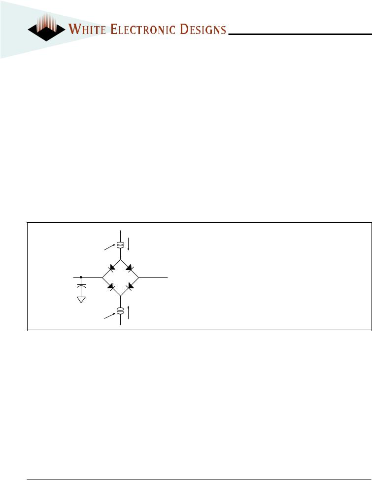
FIG. 3 |
|
AC TEST CIRCUIT |
I OL |
|
|
Current Source |
|
D.U.T. |
VZ ≈1.5V |
Ceff = 50 pf |
(Bipolar Supply) |
|
IOH
Current Source
AC TEST CONDITIONS
Parameter |
Typ |
Unit |
|
|
|
Input Pulse Levels |
VIL = 0, VIH = 3.0 |
V |
|
|
|
Input Rise and Fall |
5 |
ns |
|
|
|
Input and Output Reference Level |
1.5 |
V |
|
|
|
Output Timing Reference Level |
1.5 |
V |
|
|
|
Notes:
VZ is programmable from -2V to +7V. IOL & IOH programmable from 0 to 16mA. Tester Impedance Z0 = 75 Ω.
VZ is typically the midpoint of VOH and VOL.
IOL & IOH are adjusted to simulate a typical resistive load circuit. ATE tester includes jig capacitance.
White Electronic Designs Corporation • (602) 437-1520 • www.whiteedc.com |
4 |

|
|
|
|
|
WSF512K16-XXX |
FIG. 4 SRAM |
|
|
|
|
tRC |
TIMING WAVEFORM - READ CYCLE |
|
|
|
||
|
ADDRESS |
|
|
||
|
|
|
|
|
|
|
|
|
|
tAA |
|
|
|
|
SCS |
|
|
|
tRC |
|
|
tACS |
tCHZ |
|
|
|
|
||
ADDRESS |
|
|
|
|
|
|
|
|
tCLZ |
|
|
|
tAA |
|
|
|
|
|
|
SOE |
|
|
|
|
|
|
|
|
|
|
tOH |
|
|
tOE |
tOHZ |
|
|
|
|
tOLZ |
|
DATA I/O |
PREVIOUS DATA VALID |
DATA VALID |
DATA I/O |
HIGH IMPEDANCE |
DATA VALID |
|
|
|
|
|
|
|
READ CYCLE 1, (SCS = OE = VIL, SWE = VIH) |
|
READ CYCLE 2, (SWE = VIH) |
||
FIG. 5 SRAM
WRITE CYCLE - SWE CONTROLLED
|
tWC |
|
ADDRESS |
|
|
tAW |
|
tAH |
|
tCW |
|
|
|
|
SCS |
|
|
tAS |
tWP |
|
|
|
|
SWE |
|
tOW |
|
|
|
tWHZ |
tDW |
tDH |
DATA I/O |
DATA VALID |
|
WRITE CYCLE 1, SWE CONTROLLED
FIG. 6 SRAM
WRITE CYCLE - SCS CONTROLLED
|
tWC |
|
|
ADDRESS |
|
|
|
tAS |
tAW |
tAH |
|
tCW |
|||
|
|
||
SCS |
|
|
|
|
tWP |
|
|
SWE |
|
|
|
|
tDW |
tDH |
|
DATA I/O |
DATA VALID |
|
WRITE CYCLE 2, SCS CONTROLLED
5 |
White Electronic Designs Corporation • (602) 437-1520 • www.whiteedc.com |
 Loading...