


White Electronic Designs WSF128K16-37G1UIA, WSF128K16-37G1UI, WSF128K16-37G1UCA, WSF128K16-37G1UC, WSF128K16-72HIA Datasheet
...νAccess Times of 35ns (SRAM) and 70ns (FLASH)
νAccess Times of 70ns (SRAM) and 120ns (FLASH)
νPackaging
•66-pin, PGA Type, 1.075 inch square HIP, Hermetic Ceramic HIP (Package 400)
•66-pin, PGA Type, 1.185 inch square HIP, Hermetic Ceramic HIP (Package 401)
•68 lead, Hermetic CQFP (G1U), 22.4mm (0.880 inch) square (Package 519). Designed to fit JEDEC 68 lead 0.990” CQFJ footprint (Fig. 2)
ν128Kx16 SRAM
ν128Kx16 5V FLASH
νOrganized as 128Kx16 of SRAM and 128Kx16 of Flash Memory with separate Data Buses
νBoth blocks of memory are User Configurable as 256Kx8
νLow Power CMOS
νCommercial, Industrial and Military Temperature Ranges
νTTL Compatible Inputs and Outputs
νBuilt-in Decoupling Caps and Multiple Ground Pins for Low Noise Operation
νWeight
•WSF128K16-XHX - 13 grams typical
•WSF128K16-H1X - 13 grams typical
•WSF128K16-XG1UX - 5 grams typical
ν10,000 Erase/Program Cycles
νSector Architecture
•8 equal size sectors of 16K bytes each
•Any combination of sectors can be concurrently erased.
Also supports full chip erase
ν5 Volt Programming; 5V ± 10% Supply
νEmbedded Erase and Program Algorithms
νHardware Write Protection
νPage Program Operation and Internal Program Control Time.
Note: For programming information refer to Flash Programming 1M5 Application Note.
FIG.1 |
|
|
|
FD0-15 |
FlashDataInputs/Outputs |
|
SD0-15 |
SRAMDataInputs/Outputs |
|
A0-16 |
AddressInputs |
|
SWE1-2 |
SRAM Write Enable |
|
SCS1-2 |
SRAM Chip Selects |
|
OE |
OutputEnable |
|
VCC |
Power Supply |
|
GND |
Ground |
|
NC |
Not Connected |
|
FWE1-2 |
Flash Write Enable |
|
FCS1-2 |
Flash Chip Select |
|
|
|
May 2001 Rev. 5 |
|
White Electronic Designs Corporation • (602) 437-1520 • www.whiteedc.com |
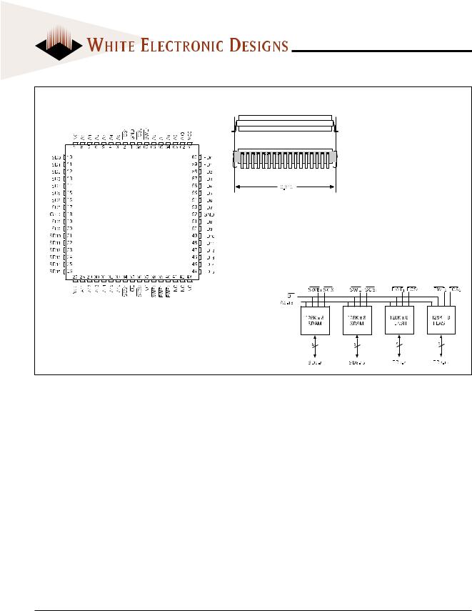
FIG. 2
The WEDC 68 lead G1U CQFP fills the same fit and function as the JEDEC 68 lead CQFJ or 68 PLCC. But the G1U has the TCE and lead inspection advantage of the CQFP form.
|
|
|
|
|
|
|
|
|
|
|
|
|
|
|
|
FD0-15 |
FlashDataInputs/Outputs |
|||
|
|
|
|
|
|
|
|
|
SD0-15 |
SRAMDataInputs/Outputs |
|||
|
|
A0-16 |
AddressInputs |
|||
|
|
|
|
|
||
|
SWE1-2 |
SRAM Write Enable |
||||
|
|
|
|
|
|
SRAM Chip Selects |
|
|
SCS1-2 |
||||
|
|
|
|
OutputEnable |
||
|
|
|
OE |
|
||
|
|
VCC |
Power Supply |
|||
|
|
GND |
Ground |
|||
|
|
NC |
Not Connected |
|||
|
|
Flash Write Enable |
||||
|
|
FWE |
1-2 |
|||
|
|
|
|
Flash Chip Select |
||
|
|
FCS1-2 |
||||
White Electronic Designs Corporation • Phoenix AZ • (602) 437-1520 |
|

|
|
|
! |
# |
! |
|
|
|
|
|
|
Operating Temperature |
T A |
-55 |
+125 |
°C |
|
StorageTemperature |
TSTG |
-65 |
+150 |
°C |
|
Signal Voltage Relative to GND |
VG |
-0.5 |
7.0 |
V |
|
Junction Temperature |
TJ |
|
|
150 |
°C |
SupplyVoltage |
VCC |
-0.5 |
7.0 |
V |
|
|
|
|
|
|
|
|
|
|
|
|
|
|
|
|
|
|
|
Flash Data Retention |
|
|
|
10 years |
|
Flash Endurance (write/erase cycles) |
|
|
10,000 |
|
|
|
|
|
|
|
|
NOTES:
1. Stresses above the absolute maximum rating may cause permanent damage to the device. Extended operation at the maximum levels may degrade performance and affect reliability.
!
|
|
! |
# |
! |
|
|
|
|
|
SupplyVoltage |
VCC |
4.5 |
5.5 |
V |
|
|
|
|
|
Input High Voltage |
VIH |
2.2 |
VCC + 0.3 |
V |
Input Low Voltage |
VIL |
-0.5 |
+0.8 |
V |
|
|
|
|
|
|
|
|
|
|
|
|
|
|
|
|
|
|
|
|
|
|
|
|
|
|
|
|
|
|
|
|
|
$% |
$& |
|||||||||||
|
|
H |
|
X |
|
X |
|
Standby |
|
High Z |
Standby |
|||||||||||
|
|
L |
|
L |
|
H |
|
Read |
|
|
Data Out |
Active |
||||||||||
|
|
L |
|
H |
|
H |
|
Read |
|
|
High Z |
Active |
||||||||||
|
|
L |
|
X |
|
L |
|
Write |
|
|
Data In |
Active |
||||||||||
|
|
|
|
|
|
|
|
|
|
|
|
|
|
|
|
|
|
|
|
|||
|
|
|
|
|
|
|
|
|
|
|
|
|
|
|
|
|
||||||
|
|
|
|
|
|
|
|
|
|
|
|
|
|
|
|
|
|
|
|
|
||
|
" |
|
|
|
|
|
|
|
|
|
|
|
! ! |
# |
! |
|||||||
|
|
|
|
|
|
|
|
|
|
|
|
|
|
|
||||||||
|
|
|
|
|
|
|
|
|
COE |
|
VIN = 0V, f = 1.0MHz |
50 |
pF |
|||||||||
|
OE |
Capacitance |
|
|
|
|
||||||||||||||||
|
|
|
|
|
|
|
|
|
|
|||||||||||||
|
F/S |
WE |
1-2 Capacitance |
|
CWE |
|
VIN = 0V, f = 1.0MHz |
20 |
pF |
|||||||||||||
|
|
|
|
|
|
|
|
|||||||||||||||
|
F/S |
CS |
1-2 Capacitance |
|
CCS |
|
VIN = 0V, f = 1.0MHz |
20 |
pF |
|||||||||||||
|
SD0-15/FD0-15 Capacitance |
|
CI/O |
|
VIN = 0V, f = 1.0MHz |
20 |
pF |
|||||||||||||||
|
A0 - A16 Capacitance |
|
|
|
CAD |
|
VIN = 0V, f = 1.0MHz |
50 |
pF |
|||||||||||||
This parameter is guaranteed by design but not tested.
|
|
|
|
|
|
|
|
|
|
|
|
|
|
|
|
|
|
|
|
|
! ! " |
! |
# |
! |
||||||
|
|
|
|
|
|
|
|
|
|
|
|
|
|
|
|
|
|
|
|
|
|
|
|
|
|
|
|
|
|
|
Input Leakage Current |
ILI |
|
VCC = 5.5, VIN = GND to VCC |
|
10 |
µA |
||||||||||||||||||||||||
|
|
|
|
|
|
|
|
|
|
|
|
|
|
|
|
|
|
|
|
|
|
|
|
|
|
|
|
|
|
|
OutputLeakageCurrent |
IL O |
|
|
|
|
= VIH, |
|
= VIH, VOUT = GND to VCC |
|
10 |
µA |
|||||||||||||||||||
|
SCS |
|
OE |
|
||||||||||||||||||||||||||
|
|
|
|
|
|
|
|
|
|
|
|
|
|
|
|
|
|
|
|
|
|
|
|
|
|
|
|
|
|
|
SRAM Operating Supply Current x 16 Mode |
ICCx16 |
|
|
|
|
|
|
|
|
= VIL, |
|
|
|
|
|
|
= |
|
|
|
= VIH, f = 5MHz, VCC = 5.5 |
|
360 |
mA |
||||||
|
|
|
SCS |
OE |
FCS |
|
||||||||||||||||||||||||
|
|
|
|
|
|
|
|
|
|
|
|
|
|
|
|
|
|
|
|
|
|
|
|
|
|
|
|
|
|
|
|
|
|
|
|
|
|
|
|
|
|
|
|
|
|
|
|
|
|
|
|||||||||||
Standby Current |
ISB |
|
|
FCS |
= |
SCS |
= VIH, |
OE |
= VIH, f = 5MHz, VCC = 5.5 |
|
40 |
mA |
||||||||||||||||||
|
|
|
|
|
|
|
|
|
|
|
|
|
|
|
|
|
|
|
|
|
|
|
|
|
|
|
|
|
|
|
SRAM Output Low Voltage |
VOL |
|
IOL = 2.1mA, VCC = 4.5 |
|
0.4 |
V |
||||||||||||||||||||||||
|
|
|
|
|
|
|
|
|
|
|
|
|
|
|
|
|
|
|
|
|
|
|
|
|
|
|
|
|
|
|
SRAM Output High Voltage |
VOH |
|
IOH = -1.0mA, VCC = 4.5 |
2.4 |
|
V |
||||||||||||||||||||||||
|
|
|
|
|
|
|
|
|
|
|
|
|
|
|
|
|
|
|
|
|
|
|
|
|
|
|
|
|
|
|
Flash VCC Active Current for Read (1) |
ICC1 |
|
|
|
|
|
= VIL, |
|
|
= |
|
= VIH |
|
100 |
mA |
|||||||||||||||
|
FCS |
OE |
SCS |
|
||||||||||||||||||||||||||
|
|
|
|
|
|
|
|
|
|
|
|
|
|
|
|
|
|
|
|
|
|
|
|
|
|
|
|
|
|
|
|
|
|
|
|
|
|
|
|
|
|
|
|
|
|
||||||||||||||||
Flash VCC Active Current for Program or |
ICC2 |
|
FCS |
= VIL, |
|
OE |
= |
SCS |
= VIH |
|
130 |
mA |
||||||||||||||||||
Erase (2) |
|
|
|
|
|
|
|
|
|
|
|
|
|
|
|
|
|
|
|
|
|
|
|
|
|
|
|
|
|
|
|
|
|
|
|
|
|
|
|
|
|
|
|
|
|
|
|
|
|
|
|
|
|
|
|
|
|
|
|
|
|
Flash Output Low Voltage |
VOL |
|
IOL = 8.0mA, VCC = 4.5 |
|
0.45 |
V |
||||||||||||||||||||||||
|
|
|
|
|
|
|
|
|
|
|
|
|
|
|
|
|
|
|
|
|
|
|
|
|
|
|
|
|
|
|
Flash Output High Voltage |
VOH1 |
|
IOH = -2.5 mA, VCC = 4.5 |
0.85 x VCC |
|
V |
||||||||||||||||||||||||
|
|
|
|
|
|
|
|
|
|
|
|
|
|
|
|
|
|
|
|
|
|
|
|
|
|
|
|
|
|
|
Flash Output High Voltage |
VOH2 |
|
IOH = -100 µA, VCC = 4.5 |
VCC -0.4 |
|
V |
||||||||||||||||||||||||
|
|
|
|
|
|
|
|
|
|
|
|
|
|
|
|
|
|
|
|
|
|
|
|
|
|
|
|
|
|
|
Flash Low VCC Lock Out Voltage |
VLKO |
|
|
|
|
|
|
|
|
|
|
|
|
|
|
|
|
|
|
|
|
|
|
|
|
|
|
3.2 |
|
V |
|
|
|
|
|
|
|
|
|
|
|
|
|
|
|
|
|
|
|
|
|
|
|
|
|
|
|
|
|
|
|
NOTES:
1.The ICC current listed includes both the DC operating current and the frequency dependent component (@ 5 MHz). The frequency component typically is less than 2 mA/MHz, with OE at VIH.
2.ICC active while Embedded Algorithm (program or erase) is in progress.
3.DC test conditions: VIL = 0.3V, VIH = VCC - 0.3V
White Electronic Designs Corporation • (602) 437-1520 • www.whiteedc.com
|
|
|
()* |
|
|
(+, |
|
! |
||
$ - |
|
! # |
! # |
|
||||||
Read Cycle Time |
tRC |
35 |
|
|
|
70 |
|
|
|
ns |
Address Access Time |
tAA |
|
35 |
|
70 |
ns |
||||
OutputHoldfromAddressChange |
tOH |
0 |
|
|
|
3 |
|
|
|
ns |
Chip Select Access Time |
tACS |
|
35 |
|
70 |
ns |
||||
Output Enable to Output Valid |
tOE |
|
20 |
|
35 |
ns |
||||
Chip Select to Output in Low Z |
tCLZ1 |
3 |
|
|
|
3 |
|
|
|
ns |
Output Enable to Output in Low Z |
tOLZ1 |
0 |
|
|
|
0 |
|
|
|
ns |
Chip Disable to Output in High Z |
tCHZ1 |
|
20 |
|
25 |
ns |
||||
OutputDisabletoOutputinHighZ |
tOHZ1 |
|
20 |
|
25 |
ns |
||||
1. This parameter is guaranteed by design but not tested.
|
|
|
()* |
|
|
(+, |
|
! |
||
!$ - |
|
! # |
|
|
|
|
|
|||
Write Cycle Time |
tWC |
35 |
|
|
|
70 |
|
|
|
ns |
Chip Select to End of Write |
tCW |
25 |
|
|
|
60 |
|
|
|
ns |
Address Valid to End of Write |
tAW |
25 |
|
|
|
60 |
|
|
|
ns |
Data Valid to End of Write |
tDW |
20 |
|
|
|
30 |
|
|
|
ns |
Write Pulse Width |
tWP |
25 |
|
|
|
50 |
|
|
|
ns |
Address Setup Time |
tAS |
0 |
|
|
|
5 |
|
|
|
ns |
Address Hold Time |
tAH |
0 |
|
|
|
5 |
|
|
|
ns |
Output Active from End of Write |
tOW1 |
4 |
|
|
|
5 |
|
|
|
ns |
Write Enable to Output in High Z |
tWHZ1 |
|
20 |
|
25 |
ns |
||||
Data Hold from Write Time |
tDH |
0 |
|
|
|
0 |
|
|
|
ns |
|
|
|
|
|
|
|
|
|
|
|
1. This parameter is guaranteed by design but not tested.
# |
|
|
|
|||||
|
|
|
|
|
|
|
|
|
|
|
|
|
|
|
. |
! |
|
|
|
|
|
|
Input Pulse Levels |
VIL = 0, VIH = 3.0 |
V |
|
|
|
|
|
|
|
|||
|
|
|
|
|
|
|
|
|
|
|
|
|
|
Input Rise and Fall |
5 |
ns |
|
|
|
|
|
|
|
|||
|
|
|
|
|
|
|
|
|
|
|
|
|
|
Input and Output Reference Level |
1.5 |
V |
|
|
|
|
|
|
|
|
|
|
|
|
|
|
|
Output Timing Reference Level |
1.5 |
V |
|
|
|
|
|
|
|
|
|
|
|
|
|
|
|
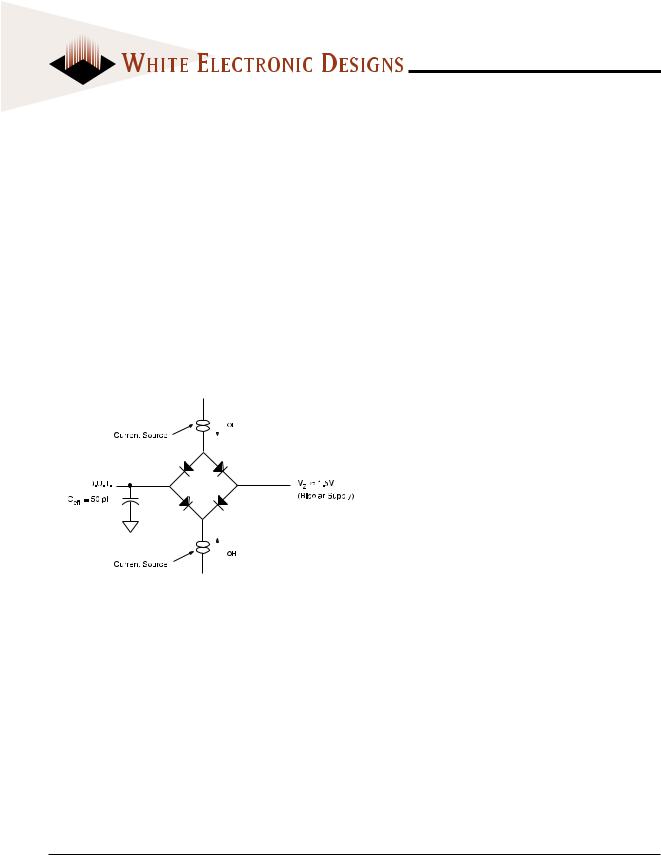
Notes: |
|
|
|
|
|
|
|
|
VZ is programmable from -2V to +7V. |
|
|
|
|
|
|
|
|
|
|
||
|
|
|
|
|
IOL & IOH programmable from 0 to 16mA. |
|
|
|
|
|
|
|
|
Tester Impedance Z0 = 75W. |
|
|
|
|
|
|
|
|
VZ is typically the midpoint of VOH and VOL. |
|
|
|
|
|
|
|
|
IOL & IOH are adjusted to simulate a typical resistive load circuit. |
|||
|
|
|
|
|
||||
|
|
|
|
|
ATE tester includes jig capacitance. |
|
|
|
|
|
|
|
|
|
|
||
|
|
|
|
|
|
|
|
|
|
|
|
|
|
|
|
|
|
White Electronic Designs Corporation • Phoenix AZ • (602) 437-1520 |
|

|
$ / ' |
'" |
'
White Electronic Designs Corporation • (602) 437-1520 • www.whiteedc.com
 Loading...