


White Electronic Designs WE512K8-300CQA, WE512K8-300CMA, WE512K8-150CQ, WE512K8-150CMA, WE512K8-150CM Datasheet
...
WE512K8, WE256K8,
WE128K8-XCX
512Kx8 CMOS EEPROM, WE512K8-XCX, SMD 5962-93091
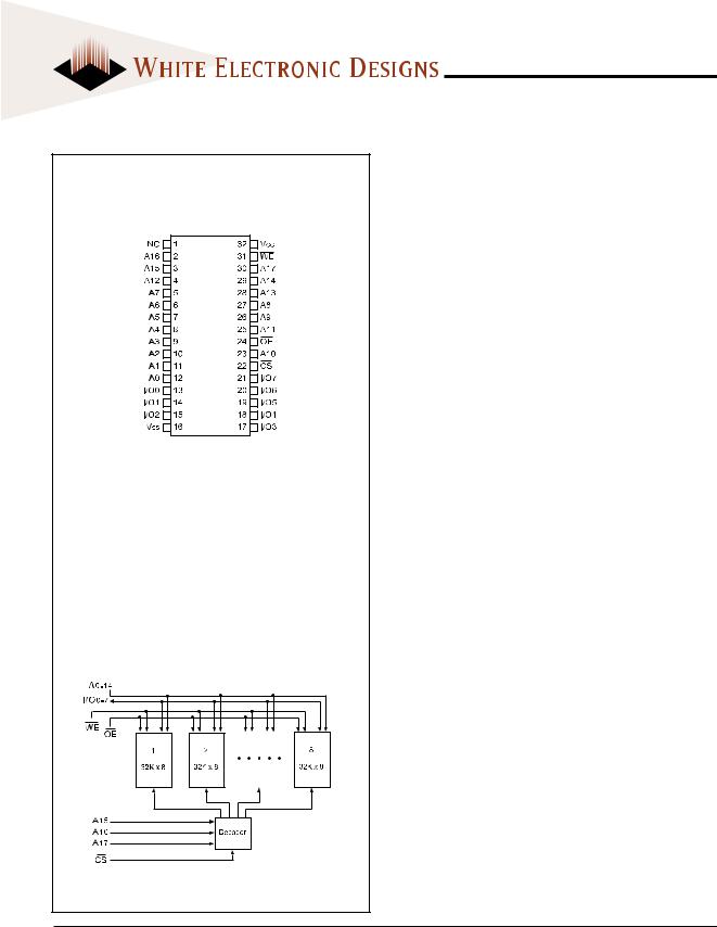
FIG. 1
PIN CONFIGURATION
TOP VIEW
|
|
|
|
|
|
|
PIN DESCRIPTION |
|
|
|
|
|
|
|
|
|
|
A0-18 |
|
Address Inputs |
||||||
|
|
|
|
|
|
|
|
|
I/O0- 7 |
|
Data Input/Output |
||||||
|
|
|
|
|
|
|
Chip Select |
|
|
CS |
|
||||||
|
|
|
Output Enable |
|||||
|
|
OE |
|
|
||||
|
|
|
|
|
|
|
Write Enable |
|
|
WE |
|
|
|||||
VCC |
|
+5.0V Power |
||||||
VSS |
|
Ground |
||||||
|
|
|
|
|
|
|
|
|
512KX8 BIT CMOS EEPROM MODULE
FEATURES
■Read Access Times of 150, 200, 250, 300ns
■JEDEC Standard 32 Pin, Hermetic Ceramic DIP (Package 300)
■Commercial, Industrial and Military Temperature Ranges
■MIL-STD-883 Compliant Devices Available
■Write Endurance 10,000 Cycles
■Data Retention at 25°C, 10 Years
■Low Power CMOS Operation:
3mA Standby Typical/100mA Operating Maximum
■Automatic Page Write Operation Internal Address and Data Latches for
512 Bytes, 1 to 128 Bytes/Row, Four Pages
■Page Write Cycle Time 10mS Max.
■Data Polling for End of Write Detection
■Hardware and Software Data Protection
■TTL Compatible Inputs and Outputs
BLOCK DIAGRAM
May 2000 Rev.1 |
1 |
White Electronic Designs Corporation • (602) 437-1520 • www.whiteedc.com |
WE512K8, WE256K8,
WE128K8-XCX
256Kx8 CMOS EEPROM, WE256K8-XCX, SMD 5962-93155
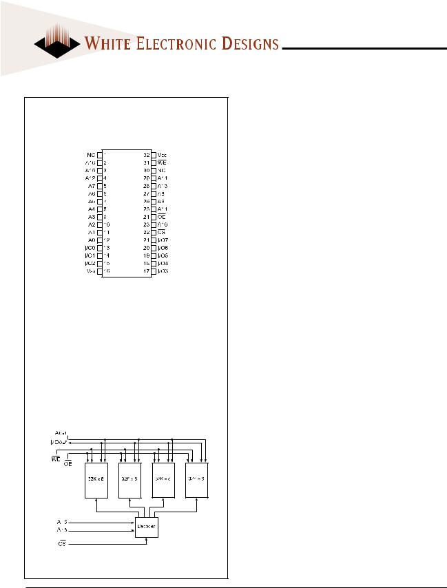
FIG.2
PIN CONFIGURATION
TOP VIEW
|
|
|
|
|
PIN DESCRIPTION |
|
|
|
|
|
|
|
|
A0-17 |
|
Address Inputs |
||||
I/O0-7 |
|
Data Input/Output |
||||
|
|
|
|
|
|
|
|
CS |
|
Chip Select |
|||
|
|
|
|
|
|
|
|
OE |
|
Output Enable |
|||
|
|
|
|
|
|
|
|
WE |
|
Write Enable |
|||
VCC |
|
+5.0V Power |
||||
VSS |
|
Ground |
||||
|
|
|
|
|
|
|
256KX8 BIT CMOS EEPROM MODULE
FEATURES
■Read Access Times of 150, 200ns
■JEDEC Standard 32 Pin, Hermetic Ceramic DIP (Package 302)
■Commercial, Industrial and Military Temperature Ranges
■MIL-STD-883 Compliant Devices Available
■Write Endurance 10,000 Cycles
■Data Retention at 25°C, 10 Years
■Low Power CMOS Operation:
2mA Standby Typical/90mA Operating Maximum
■Automatic Page Write Operation Internal Address and Data Latches for
512 Bytes, 1 to 64 Bytes/Row, Eight Pages
■Page Write Cycle Time 10mS Max.
■Data Polling for End of Write Detection
■Hardware and Software Data Protection
■TTL Compatible Inputs and Outputs
BLOCK DIAGRAM
White Electronic Designs Corporation • Phoenix AZ • (602) 437-1520 |
2 |
WE512K8, WE256K8,
WE128K8-XCX
128Kx8 CMOS EEPROM, WE128K8-XCX, SMD 5962-93154
FIG. 3
PIN CONFIGURATION
TOP VIEW
|
|
|
|
|
|
|
PIN DESCRIPTION |
|
|
|
|
|
|
|
|
|
|
A0-16 |
|
Address Inputs |
||||||
I/O0-7 |
|
Data Input/Output |
||||||
|
|
|
|
|
Chip Select |
|||
|
|
|
CS |
|
|
|
||
|
|
|
|
|
|
|||
|
OE |
|
Output Enable |
|||||
|
|
|
|
|
|
|
|
|
|
WE |
|
Write Enable |
|||||
VCC |
|
+5.0V Power |
||||||
VSS |
|
Ground |
||||||
128KX8 BIT CMOS EEPROM MODULE
FEATURES
■Read Access Times of 150, 200ns
■JEDEC Standard 32 Pin, Hermetic Ceramic DIP (Package 300)
■Commercial, Industrial and Military Temperature Ranges
■MIL-STD-883 Compliant Devices Available
■Write Endurance 10,000 Cycles
■Data Retention at 25°C, 10 Years
■Low Power CMOS Operation:
1mA Standby Typical/70mA Operating
■Automatic Page Write Operation Internal Address and Data Latches for
256 Bytes, 1 to 64 Bytes/Row, Four Pages
■Page Write Cycle Time 10mS Max.
■Data Polling for End of Write Detection
■Hardware and Software Data Protection
■TTL Compatible Inputs and Outputs
BLOCK DIAGRAM
3White Electronic Designs Corporation • (602) 437-1520 • www.whiteedc.com
WE512K8, WE256K8, WE128K8-XCX
ABSOLUTE MAXIMUM RATINGS
Parameter |
Symbol |
|
Unit |
Operating Temperature |
TA |
-55 to +125 |
°C |
Storage Temperature |
TSTG |
-65 to +150 |
°C |
Signal Voltage Any Pin |
VG |
-0.6 to + 6.25 |
V |
Voltage on OE and A9 |
|
-0.6 to +13.5 |
V |
Thermal Resistance |
qJC |
28 |
°C/W |
junction to case |
|
|
|
Lead Temperature |
|
+300 |
°C |
(soldering -10 secs) |
|
|
|
|
|
|
|
NOTE:
Stresses above those listed under "Absolute Maximum Ratings" may cause permanent damage to the device. This is a stress rating only and functional operation of the device at these or any other conditions above those indicated in the operational sections of this specification is not implied. Exposure to absolute maximum rating conditions for extended periods may affect device reliability.
RECOMMENDED OPERATING CONDITIONS
Parameter |
Symbol |
Min |
Max |
Unit |
|
|
|
|
|
Supply Voltage |
VCC |
4.5 |
5.5 |
V |
Input High Voltage |
VIH |
2.0 |
VCC + 0.3 |
V |
Input Low Voltage |
VIL |
-0.3 |
+0.8 |
V |
Operating Temp. (Mil.) |
TA |
-55 |
+125 |
°C |
|
|
|
|
|
Operating Temp. (Ind.) |
TA |
-40 |
+85 |
°C |
|
|
|
|
|
TRUTH TABLE
|
|
|
|
|
|
|
|
|
|
|
CS |
OE |
|
|
WE |
Mode |
Data I/O |
||||
|
|
|
|
|
|
|
|
|
|
|
|
H |
|
X |
|
|
X |
Standby |
High Z |
||
|
L |
|
L |
|
|
H |
Read |
Data Out |
||
|
L |
|
H |
|
|
L |
Write |
Data In |
||
|
X |
|
H |
|
|
X |
Out Disable |
High Z/Data Out |
||
|
X |
|
X |
|
|
H |
Write |
|
||
|
X |
|
L |
|
|
X |
Inhibit |
|
||
CAPACITANCE
(TA = +25°C)
Parameter |
Sym |
Condition |
512Kx8 |
256Kx8 |
128Kx8 |
Unit |
|
|
|
Max |
Max |
Max |
|
Input Capacitance |
CIN |
VIN = 0V, f = 1MHz |
45 |
80 |
45 |
pF |
Output Capacitance |
COUT |
VI/O = 0V, f = 1MHz |
60 |
80 |
60 |
pF |
This parameter is guaranteed by design but not tested.
DC CHARACTERISTICS
(VCC = 5.0V, VSS = 0V, TA = -55°C TO +125°C)
Parameter |
Symbol |
Conditions |
512K x 8 |
256K x 8 |
|
128K x 8 |
Unit |
|||||||||||||
|
|
|
|
|
|
|
|
|
|
Min |
Typ |
Max |
Min |
Typ |
Max |
Min |
|
Typ |
Max |
|
Input Leakage Current |
ILI |
VCC = 5.5, VIN = GND to VCC |
|
|
10 |
|
|
10 |
|
|
|
10 |
µA |
|||||||
Output Leakage Current |
ILO |
|
|
= VIH, |
|
|
= VIH, VOUT = GND to VCC |
|
|
10 |
|
|
10 |
|
|
|
10 |
µA |
||
|
CS |
|
OE |
|
|
|
|
|
|
|
||||||||||
|
|
|
|
|
|
|
|
|
|
|
|
|
|
|
|
|
||||
Dynamic Supply Current |
ICC |
CS = VIL, OE = VIH, f = 5MHz, VCC = 5.5 |
|
80 |
100 |
|
60 |
90 |
|
|
50 |
70 |
mA |
|||||||
|
|
|
|
|
|
|
|
|
|
|
|
|
|
|
|
|
|
|||
Standby Current |
ISB |
CS = VIL, OE = VIH, f = 5MHz, VCC = 5.5 |
|
3 |
8 |
|
2 |
6 |
|
|
1 |
4 |
mA |
|||||||
Output Low Voltage |
VOL |
IOL = 2.1mA, VCC = 4.5V |
|
|
0.45 |
|
|
0.45 |
|
|
|
0.45 |
V |
|||||||
Output High Voltage |
VOH |
IOH = -400µA, VCC = 4.5V |
2.4 |
|
|
2.4 |
|
|
2.4 |
|
|
|
V |
|||||||
NOTE: DC test conditions: VIH = VCC -0.3V, VIL = 0.3V
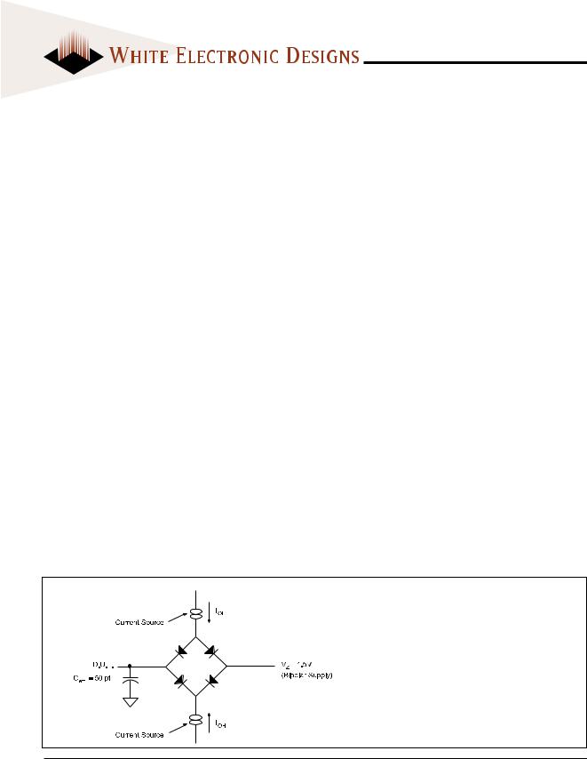
FIG. 4
AC TEST CIRCUIT
AC TEST CONDITIONS
Parameter |
Typ |
Unit |
|
|
|
Input Pulse Levels |
VIL = 0, VIH = 3.0 |
V |
Input Rise and Fall |
5 |
ns |
Input and Output Reference Level |
1.5 |
V |
Output Timing Reference Level |
1.5 |
V |
Notes:
VZ is programmable from -2V to +7V. IOL & IOH programmable from 0 to 16mA. Tester Impedance Z0 = 75 ý.
VZ is typically the midpoint of VOH and VOL.
IOL & IOH are adjusted to simulate a typical resistive load circuit. ATE tester includes jig capacitance.
White Electronic Designs Corporation • Phoenix AZ • (602) 437-1520 |
4 |
 Loading...