


White Electronic Designs WF2M32U-150HI5A, WF2M32U-150HI5, WF2M32U-150HC5A, WF2M32U-150HC5, WF2M32U-150G2UM5A Datasheet
...
WF2M32-XXX5
2Mx32 5V FLASH MODULE, SMD 5962-97531 (pending)
FEATURES
HI-RELIABILITY PRODUCT
PRELIMINARY*
■Access Time of 90, 120, 150ns
■Packaging:
•66 pin, PGA Type, 1.185" square, Hermetic Ceramic HIP (Package 401).
•68 lead, Hermetic CQFP (G2U), 22.4mm (0.880") square (Package 510) 3.56mm (0.140") height. Designed to fit JEDEC 68 lead 0.990" CQFJ footprint (Fig. 3)
■Sector Architecture
•32 equal size sectors of 64KBytes per each 2Mx8 chip
•Any combination of sectors can be erased. Also supports full chip erase.
■Minimum 100,000 Write/Erase Cycles Minimum
■Organized as 2Mx32
■Commercial, Industrial, and Military Temperature Ranges
■5 Volt Read and Write. 5V ± 10% Supply.
■Low Power CMOS
■Data Polling and Toggle Bit feature for detection of program or erase cycle completion.
■Supports reading or programming data to a sector not being erased.
■RESET pin resets internal state machine to the read mode.
■Built in Decoupling Caps and Multiple Ground Pins for Low Noise Operation, Separate Power and Ground Planes to improve noise immunity
*This data sheet describes a product under development, not fully characterized, and is subject to change without notice.
Note: For programming information refer to Flash Programming 16M5 Application Note.
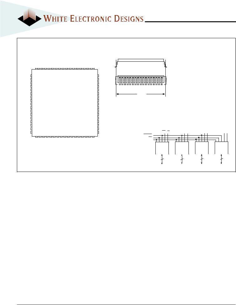
FIG. 1 PIN CONFIGURATION FOR WF2M32-XHX5 |
|
|
|
|
|||||||
|
|
TOP VIEW |
|
|
|
|
|
|
PIN DESCRIPTION |
||
1 |
12 |
23 |
|
34 |
45 |
|
56 |
|
|
I/O0-31 |
Data Inputs/Outputs |
|
|
|
|
A0-20 |
Address Inputs |
||||||
|
|
|
|
|
|
|
|
|
|
||
I/O8 |
WE2 |
I/O15 |
I/O24 |
|
VCC |
I/O31 |
|
|
|
WE1-4 |
Write Enables |
|
|
|
|
|
|
|
|
|
|
||
I/O9 |
CS2 |
I/O14 |
I/O25 |
|
CS4 |
I/O30 |
|
|
|
CS1-4 |
Chip Selects |
I/O10 |
GND |
I/O13 |
I/O26 |
|
WE4 |
I/O29 |
|
|
|
OE |
Output Enable |
|
|
|
|
VCC |
Power Supply |
||||||
|
|
|
|
|
|
|
|
|
|
||
A14 |
I/O11 |
I/O12 |
A7 |
|
I/O27 |
I/O28 |
|
|
|
GND |
Ground |
|
|
|
|
|
|
|
|
|
|
||
A16 |
A10 |
OE |
A12 |
|
A4 |
A1 |
|
|
|
|
|
A11 |
A9 |
A17 |
A20 |
|
A5 |
A2 |
|
|
BLOCK DIAGRAM |
|
|
|
|
|
|
|
|
||||||
A0 |
A15 |
WE1 |
A13 |
|
A6 |
A3 |
|
WE1 CS1 |
WE2 CS2 |
WE3 CS3 |
WE4 CS4 |
|
OE |
|
|
|
|
||||||
|
|
|
|
|
|
|
|
|
|
|
|
|
VCC |
I/O7 |
|
|
WE3 |
I/O23 |
A 0 - 20 |
|
|
|
|
A18 |
A8 |
|
|
|
|
|
|
||||
I/O0 |
CS1 |
I/O6 |
I/O16 |
|
CS3 |
I/O22 |
|
2M x 8 |
2M x 8 |
2M x 8 |
2M x 8 |
|
|
|
|
|
|
||||||
I/O1 |
A19 |
I/O5 |
I/O17 |
|
GND |
I/O21 |
|
|
|
|
|
|
|
|
|
|
|
|
|
8 |
8 |
8 |
8 |
I/O2 |
I/O3 |
I/O4 |
I/O18 |
|
I/O19 |
I/O20 |
|
|
|
|
|
11 |
22 |
33 |
|
44 |
55 |
|
66 |
I/O 0 - 7 |
I/O 8 - 15 |
I/O 16 - 23 |
I/O 24 - 31 |
|
|
|
|
|
|
||||||
RESET internally tied to Vcc in the HIP package for this pin configuration. See Alternate Pin Configuration with RESET tied to pin 12 for system control of reset (Fig. 10, page 11)
October 1999 Rev.3 |
1 |
White Electronic Designs Corporation • Phoenix, AZ • (602) 437-1520 |
WF2M32-XXX5
FIG. 2 PIN CONFIGURATION FOR WF2M32-XG2UX5
TOP VIEW
|
|
RESET |
A0 |
A1 |
A2 |
A3 |
A4 |
A5 |
|
CS3 |
|
GND |
|
CS4 |
|
WE1 A6 A7 |
|
A8 |
A9 |
A10 |
VCC |
|
||||
|
|
|
|
|
|
|||||||||||||||||||||
|
9 |
8 |
7 |
6 |
5 |
4 |
3 |
2 |
1 |
68 67 66 65 64 63 62 61 |
|
|||||||||||||||
I/O0 |
10 |
|
|
|
|
|
|
|
|
|
|
|
|
|
|
|
|
|
|
|
|
|
|
|
60 |
I/O16 |
I/O1 |
11 |
|
|
|
|
|
|
|
|
|
|
|
|
|
|
|
|
|
|
|
|
|
|
|
59 |
I/O17 |
I/O2 |
12 |
|
|
|
|
|
|
|
|
|
|
|
|
|
|
|
|
|
|
|
|
|
|
|
58 |
I/O18 |
I/O3 |
13 |
|
|
|
|
|
|
|
|
|
|
|
|
|
|
|
|
|
|
|
|
|
|
|
57 |
I/O19 |
I/O4 |
14 |
|
|
|
|
|
|
|
|
|
|
|
|
|
|
|
|
|
|
|
|
|
|
|
56 |
I/O20 |
I/O5 |
15 |
|
|
|
|
|
|
|
|
|
|
|
|
|
|
|
|
|
|
|
|
|
|
|
55 |
I/O21 |
I/O6 |
16 |
|
|
|
|
|
|
|
|
|
|
|
|
|
|
|
|
|
|
|
|
|
|
|
54 |
I/O22 |
I/O7 |
17 |
|
|
|
|
|
|
|
|
|
|
|
|
|
|
|
|
|
|
|
|
|
|
|
53 |
I/O23 |
GND |
18 |
|
|
|
|
|
|
|
|
|
|
|
|
|
|
|
|
|
|
|
|
|
|
|
52 |
GND |
I/O8 |
19 |
|
|
|
|
|
|
|
|
|
|
|
|
|
|
|
|
|
|
|
|
|
|
|
51 |
I/O24 |
I/O9 |
20 |
|
|
|
|
|
|
|
|
|
|
|
|
|
|
|
|
|
|
|
|
|
|
|
50 |
I/O25 |
I/O10 |
21 |
|
|
|
|
|
|
|
|
|
|
|
|
|
|
|
|
|
|
|
|
|
|
|
49 |
I/O26 |
I/O11 |
22 |
|
|
|
|
|
|
|
|
|
|
|
|
|
|
|
|
|
|
|
|
|
|
|
48 |
I/O27 |
I/O12 |
23 |
|
|
|
|
|
|
|
|
|
|
|
|
|
|
|
|
|
|
|
|
|
|
|
47 |
I/O28 |
I/O13 |
24 |
|
|
|
|
|
|
|
|
|
|
|
|
|
|
|
|
|
|
|
|
|
|
|
46 |
I/O29 |
I/O14 |
25 |
|
|
|
|
|
|
|
|
|
|
|
|
|
|
|
|
|
|
|
|
|
|
|
45 |
I/O30 |
I/O15 |
26 |
|
|
|
|
|
|
|
|
|
|
|
|
|
|
|
|
|
|
|
|
|
|
|
44 |
I/O31 |
|
27 28 29 30 31 32 33 34 35 36 37 38 39 40 41 42 43 |
|
||||||||||||||||||||||||
|
|
VCC |
A11 |
A12 |
A13 |
A14 |
A15 |
A16 |
|
CS1 |
|
OE |
|
CS2 |
|
A17 |
|
WE2 |
|
WE3 |
|
WE4 |
A18 |
A19 |
A20 |
|
|
|
|
|
|
|
|
||||||||||||||||||||
0.940"
The White 68 lead G2U CQFP fills the same fit and function as the JEDEC 68 lead CQFJ or 68 PLCC. But the G2U has the TCE and lead inspection advantage of the CQFP form.
WE1 CS 1
RESET
OE
A 0 - 2 0
PIN DESCRIPTION
|
|
I/O0-31 |
Data Inputs/Outputs |
||||||
|
|
|
A0-20 |
Address Inputs |
|||||
|
|
|
|
|
|
|
|
|
|
|
|
|
|
|
|
Write Enables |
|||
|
|
WE |
1-4 |
|
|||||
|
|
|
|
|
|
|
|
|
|
|
|
|
|
|
Chip Selects |
||||
|
|
|
CS |
1-4 |
|
||||
|
|
|
|
|
|
|
|
|
|
|
|
|
|
|
|
|
Output Enable |
||
|
|
|
|
OE |
|
|
|||
|
|
|
|
|
|
|
|
|
|
|
|
|
VCC |
Power Supply |
|||||
|
|
|
|
|
|
|
|
|
|
|
|
|
GND |
Ground |
|||||
|
|
|
|
|
|
|
|
|
|
|
|
Reset |
|||||||
|
RESET |
|
|||||||
BLOCK DIAGRAM
|
|
|
|
|
|
|
|
|
|
|
|
|
WE2 CS 2 |
WE3 CS 3 |
WE4 CS4 |
||||||||||
2M x 8 |
|
2M x 8 |
|
2M x 8 |
|
2M x 8 |
|
|
|
|
|
|
|
8 |
8 |
8 |
8 |
|||
I/O 0 - 7 |
|
I/O 8 - 1 5 |
|
I/O 1 6 - 2 3 |
|
I/O 2 4 - 3 1 |
White Electronic Designs Corporation • Phoenix, AZ • (602) 437-1520 |
2 |

WF2M32-XXX5
ABSOLUTE MAXIMUM RATINGS
Parameter |
Symbol |
Ratings |
Unit |
Voltage on Any Pin Relative to VSS |
VT |
-2.0 to +7.0 |
V |
Power Dissipation |
PT |
8 |
W |
Storage Temperature |
Tstg |
-65 to +125 |
°C |
Short Circuit Output Current |
IOS |
100 |
mA |
Endurance - Write/Erase Cycles |
|
100,000 min |
cycles |
(Mil Temp) |
|
|
|
Data Retention (Mil Temp) |
|
20 |
years |
|
|
|
|
RECOMMENDED DC OPERATING CONDITIONS
Parameter |
Symbol |
Min |
Typ |
Max |
Unit |
|
|
|
|
|
|
Supply Voltage |
VCC |
4.5 |
5.0 |
5.5 |
V |
Ground |
VSS |
0 |
0 |
0 |
V |
Input High Voltage |
VIH |
2.0 |
- |
VCC + 0.5 |
V |
Input Low Voltage |
VIL |
-0.5 |
- |
+0.8 |
V |
Operating Temperature (Mil.) |
TA |
-55 |
- |
+125 |
°C |
Operating Temperature (Ind.) |
TA |
-40 |
- |
+85 |
°C |
CAPACITANCE
(TA = +25°C)
|
Parameter |
Symbol |
Conditions |
Max |
Unit |
|||||||
|
|
|
|
|
|
|
|
|
|
|
|
|
|
|
|
|
|
capacitance |
COE |
VIN = 0 V, f = 1.0 MHz |
50 |
pF |
|||
|
OE |
|
||||||||||
|
|
|
|
|
1-4 capacitance |
CWE |
VIN = 0 V, f = 1.0 MHz |
|
pF |
|||
|
WE |
|
||||||||||
|
|
|
|
|
HIP (PGA) |
|
|
20 |
|
|||
|
|
|
|
|
HIP (Alternate pinout) |
|
|
|
|
50 |
|
|
|
|
|
|
|
CQFP G4T |
|
|
|
|
50 |
|
|
|
|
|
|
|
CQFP G2U |
|
|
|
20 |
|
||
|
|
|
|
|
G2 (Alternate pinout) |
|
|
|
50 |
|
||
|
|
|
1-4 capacitance |
CCS |
VIN = 0 V, f = 1.0 MHz |
20 |
pF |
|||||
|
CS |
|||||||||||
|
Data I/O capacitance |
CI/O |
VI/O = 0 V, f = 1.0 MHz |
20 |
pF |
|||||||
|
Address input capacitance |
CAD |
VIN = 0 V, f = 1.0 MHz |
50 |
pF |
|||||||
This parameter is guaranteed by design but not tested.
DC CHARACTERISTICS - CMOS COMPATIBLE
(VCC = 5.0V, VSS = 0V, TA = -55°C to +125°C)
Parameter |
Symbol |
|
|
|
|
|
|
|
|
|
Conditions |
Min |
Max |
Unit |
||
Input Leakage Current |
ILI |
|
VCC = 5.5, VIN = GND to VCC |
|
10 |
A |
||||||||||
Output Leakage Current |
ILOx32 |
|
VCC = 5.5, VIN = GND to VCC |
|
10 |
A |
||||||||||
VCC Active Current for Read (1) |
ICC1 |
|
|
|
|
|
|
= VIH, f = 5MHz |
|
160 |
mA |
|||||
|
CS |
= VIL, |
OE |
|
|
|||||||||||
VCC Active Current for Program or Erase (2) |
ICC2 |
|
|
|
|
|
|
|
= VIH |
|
240 |
mA |
||||
|
CS |
= VIL, |
OE |
|
||||||||||||
|
|
|
|
|
|
|
|
|
|
|
||||||
VCC Standby Current |
ICC3 |
|
VCC = 5.5, |
CS |
= VIH, f = 5MHz, |
RESET |
= Vcc ± 0.3V |
|
8.0 |
mA |
||||||
Output Low Voltage |
VOL |
|
IOL = 12.0 mA, VCC = 4.5 |
|
0.45 |
V |
||||||||||
Output High Voltage |
VOH |
|
IOH = -2.5 mA, VCC = 4.5 |
0.85xVcc |
|
V |
||||||||||
Low VCC Lock-Out Voltage |
VLKO |
|
|
|
|
|
|
|
|
|
|
|
|
3.2 |
4.2 |
V |
|
|
|
|
|
|
|
|
|
|
|
|
|
|
|
|
|
NOTES:
1.The Icc current listed includes both the DC operating current and the frequency dependent component (@ 5MHz). The frequency component typically is less than 2mA/MHz, with OE at VIH.
2.Icc active while Embedded Algorithm (program or erase) is in progress.
3.DC test conditions VIL = 0.3V, VIH = VCC - 0.3V
3 |
White Electronic Designs Corporation • Phoenix, AZ • (602) 437-1520 |

WF2M32-XXX5
AC CHARACTERISTICS – WRITE/ERASE/PROGRAM OPERATIONS - WE CONTROLLED
(VCC = 5.0V, TA = -55°C to +125°C)
|
Parameter |
Symbol |
-90 |
|
|
-120 |
|
-150 |
Unit |
||||||
|
|
|
|
|
Min |
Max |
Min |
|
Max |
Min |
|
Max |
|
|
|
|
Write Cycle Time |
tAVAV |
tWC |
90 |
|
|
120 |
|
|
150 |
|
|
ns |
||
|
|
|
|
|
|
|
|
|
|
|
|
|
|
|
|
|
Chip Select Setup Time |
tELWL |
tCS |
0 |
|
|
0 |
|
|
0 |
|
|
ns |
||
|
|
|
|
|
|
|
|
|
|
|
|
|
|
|
|
|
Write Enable Pulse Width |
tWLWH |
tWP |
45 |
|
|
50 |
|
|
50 |
|
|
ns |
||
|
|
|
|
|
|
|
|
|
|
|
|
|
|
|
|
|
Address Setup Time |
tAVWL |
tAS |
0 |
|
|
0 |
|
|
0 |
|
|
ns |
||
|
|
|
|
|
|
|
|
|
|
|
|
|
|
|
|
|
Data Setup Time |
tDVWH |
tDS |
45 |
|
|
50 |
|
|
50 |
|
|
ns |
||
|
|
|
|
|
|
|
|
|
|
|
|
|
|
|
|
|
Data Hold Time |
tWHDX |
tDH |
0 |
|
|
0 |
|
|
0 |
|
|
ns |
||
|
|
|
|
|
|
|
|
|
|
|
|
|
|
|
|
|
Address Hold Time |
tWLAX |
tAH |
45 |
|
|
50 |
|
|
50 |
|
|
ns |
||
|
|
|
|
|
|
|
|
|
|
|
|
|
|
|
|
|
Write Enable Pulse Width High |
tWHWL |
tWPH |
20 |
|
|
20 |
|
|
20 |
|
|
ns |
||
|
|
|
|
|
|
|
|
|
|
|
|
|
|
|
|
|
Duration of Byte Programming Operation (1) |
tWHWH1 |
|
|
|
300 |
|
|
300 |
|
|
300 |
s |
|
|
|
|
|
|
|
|
|
|
|
|
|
|
|
|
|
|
|
Sector Erase (2) |
tWHWH2 |
|
|
|
15 |
|
|
15 |
|
|
15 |
sec |
||
|
|
|
|
|
|
|
|
|
|
|
|
|
|
|
|
|
Read Recovery Time before Write |
tGHWL |
|
0 |
|
|
0 |
|
|
0 |
|
|
s |
|
|
|
|
|
|
|
|
|
|
|
|
|
|
|
|
|
|
|
VCC Setup Time |
tVCS |
|
50 |
|
|
50 |
|
|
50 |
|
|
s |
|
|
|
|
|
|
|
|
|
|
|
|
|
|
|
|
|
|
|
Chip Programming Time |
|
|
|
|
44 |
|
|
44 |
|
|
44 |
sec |
||
|
|
|
|
|
|
|
|
|
|
|
|
|
|
|
|
|
Chip Erase Time (3) |
|
|
|
|
256 |
|
|
256 |
|
|
256 |
sec |
||
|
|
|
|
|
|
|
|
|
|
|
|
|
|
|
|
|
Output Enable Hold Time (4) |
|
tOEH |
10 |
|
|
10 |
|
|
10 |
|
|
ns |
||
|
|
|
|
|
|
|
|
|
|
|
|
|
|
|
|
|
|
|
tRP |
500 |
|
|
500 |
|
|
500 |
|
|
ns |
||
|
RESET |
Pulse Width (5) |
|
|
|
|
|
|
|
||||||
|
|
|
|
|
|
|
|
|
|
|
|
|
|
|
|
NOTES:
1.Typical value for tWHWH1 is 7 s.
2.Typical value for tWHWH2 is 1sec.
3.Typical value for Chip Erase Time is 32sec.
4.For Toggle and Data Polling.
5.RESET internally tied to Vcc for the default pin configuration in the HIP package.
AC CHARACTERISTICS – READ-ONLY OPERATIONS
(VCC = 5.0V, TA = -55°C to +125°C)
Parameter |
Symbol |
|
-90 |
|
-120 |
|
-150 |
Unit |
|||||||||
|
|
|
|
|
|
|
Min |
|
Max |
Min |
|
Max |
Min |
|
Max |
|
|
|
|
|
|
|
|
|
|
|
|
|
|
|
|
|
|
|
|
Read Cycle Time |
tAVAV |
tRC |
90 |
|
|
120 |
|
|
150 |
|
|
ns |
|||||
|
|
|
|
|
|
|
|
|
|
|
|
|
|
|
|
|
|
Address Access Time |
tAVQV |
tACC |
|
|
90 |
|
|
120 |
|
|
150 |
ns |
|||||
|
|
|
|
|
|
|
|
|
|
|
|
|
|
|
|
|
|
Chip Select Access Time |
tELQV |
tCE |
|
|
90 |
|
|
120 |
|
|
150 |
ns |
|||||
|
|
|
|
|
|
|
|
|
|
|
|
|
|
|
|
|
|
Output Enable to Output Valid |
tGLQV |
tOE |
|
|
40 |
|
|
50 |
|
|
55 |
ns |
|||||
|
|
|
|
|
|
|
|
|
|
|
|
|
|
|
|
|
|
Chip Select High to Output High Z (1) |
tEHQZ |
tDF |
|
|
20 |
|
|
30 |
|
|
35 |
ns |
|||||
|
|
|
|
|
|
|
|
|
|
|
|
|
|
|
|
|
|
Output Enable High to Output High Z (1) |
tGHQZ |
tDF |
|
|
20 |
|
|
30 |
|
|
35 |
ns |
|||||
|
|
|
|
|
|
|
|
|
|
|
|
|
|
|
|
|
|
|
|
|
|
|
|
|
|
|
|
|
|
|
|
|
|||
Output Hold from Addresses, |
CS |
or |
OE |
Change, |
tAXQX |
tOH |
0 |
|
|
0 |
|
|
0 |
|
|
ns |
|
whichever is First |
|
|
|
|
|
|
|
|
|
|
|
|
|
||||
|
|
|
|
|
|
|
|
|
|
|
|
|
|
|
|
|
|
RST Low to Read Mode (1,2) |
|
tReady |
|
|
20 |
|
|
20 |
|
|
20 |
s |
|
||||
1.Guaranteed by design, not tested.
2.RESET internally tied to Vcc for the default pin configuration in the HIP package.
White Electronic Designs Corporation • Phoenix, AZ • (602) 437-1520 |
4 |
WF2M32-XXX5
AC CHARACTERISTICS – WRITE/ERASE/PROGRAM OPERATIONS,CS CONTROLLED
(VCC = 5.0V, VSS = 0V, TA = -55°C to +125°C)
Parameter |
Symbol |
|
-90 |
|
|
-120 |
|
-150 |
Unit |
||||
|
|
|
|
Min |
Max |
Min |
|
Max |
Min |
|
Max |
|
|
Write Cycle Time |
tAVAV |
|
tWC |
90 |
|
|
120 |
|
|
150 |
|
|
ns |
Write Enable Setup Time |
tWLEL |
|
tWS |
0 |
|
|
0 |
|
|
0 |
|
|
ns |
Chip Select Pulse Width |
tELEH |
|
tCP |
45 |
|
|
50 |
|
|
50 |
|
|
ns |
Address Setup Time |
tAVEL |
|
tAS |
0 |
|
|
0 |
|
|
0 |
|
|
ns |
Data Setup Time |
tDVEH |
|
tDS |
45 |
|
|
50 |
|
|
50 |
|
|
ns |
Data Hold Time |
tEHDX |
|
tDH |
0 |
|
|
0 |
|
|
0 |
|
|
ns |
Address Hold Time |
tELAX |
|
tAH |
45 |
|
|
50 |
|
|
50 |
|
|
ns |
Chip Select Pulse Width High |
tEHEL |
|
tCPH |
20 |
|
|
20 |
|
|
20 |
|
|
ns |
Duration of Byte Programming Operation (1) |
tWHWH1 |
|
|
|
|
300 |
|
|
300 |
|
|
300 |
µs |
Sector Erase Time (2) |
tWHWH2 |
|
|
|
|
15 |
|
|
15 |
|
|
15 |
sec |
Read Recovery Time |
tGHEL |
|
|
0 |
|
|
0 |
|
|
0 |
|
|
µs |
Chip Programming Time |
|
|
|
|
|
44 |
|
|
44 |
|
|
44 |
sec |
Chip Erase Time (3) |
|
|
|
|
|
256 |
|
|
256 |
|
|
256 |
sec |
Output Enable Hold Time (4) |
|
|
tOEH |
10 |
|
|
10 |
|
|
10 |
|
|
ns |
|
|
|
|
|
|
|
|
|
|
|
|
|
|
NOTES:
1.Typical value for tWHWH1 is 7µs.
2.Typical value for tWHWH2 is 1sec.
3.Typical value for Chip Erase Time is 32sec.
4.For Toggle and Data Polling.
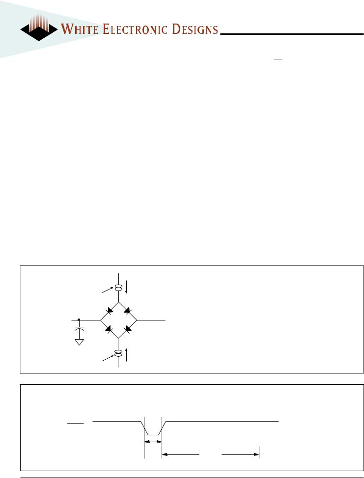
FIG. 3
AC TEST CIRCUIT I OL
Current Source
D.U.T.
Ceff = 50 pf
CS
IOH
Current Source
AC TEST CONDITIONS
|
Parameter |
Typ |
Unit |
|
Input Pulse Levels |
VIL = 0, VIH = 3.0 |
V |
|
|
|
|
|
Input Rise and Fall |
5 |
ns |
|
Input and Output Reference Level |
1.5 |
V |
VZ ≈1.5V |
Output Timing Reference Level |
1.5 |
V |
(Bipolar Supply)
NOTES:
VZ is programmable from -2V to +7V. IOL & IOH programmable from 0 to 16mA. Tester Impedance Z0 = 75 Ω.
VZ is typically the midpoint of VOH and VOL.
IOL & IOH are adjusted to simulate a typical resistive load circuit. The risingATE testeredgeincludesof the lastjig capacitanceWE signal.
|
WE |
|
Entire programming |
FIG. 4 |
or erase operations |
RESET TIMINGRY/BYDIAGRAM
tBUSY
RESET
tRP
tReady
5 |
White Electronic Designs Corporation • Phoenix, AZ • (602) 437-1520 |
 Loading...