


White Electronic Designs WEDPND16M72S-266BM, WEDPND16M72S-266BI, WEDPND16M72S-266BC, WEDPND16M72S-250BM, WEDPND16M72S-250BI Datasheet
... White Electronic Designs WEDPND16M72S-XBX
16Mx72 DDR SDRAM Preliminary*
FEATURES
νHigh Frequency = 200, 250, 266MHz
νPackage:
• 219 Plastic Ball Grid Array (PBGA), 32 x 25mm
ν2.5V ±0.2V core power supply
ν2.5V I/O (SSTL_2 compatible)
νDifferential clock inputs (CLK and CLK)
νCommands entered on each positive CLK edge
νInternal pipelined double-data-rate (DDR) architecture; two data accesses per clock cycle
νProgrammable Burst length: 2,4 or 8
νBidirectional data strobe (DQS) transmitted/received with data, i.e., source-synchronous data capture (one per byte)
νDQS edge-aligned with data for READs; center-aligned with data for WRITEs
νDLL to align DQ and DQS transitions with CLK
νFour internal banks for concurrent operation
νTwo data mask (DM) pins for masking write data
νProgrammable IOL/IOH option
νAuto precharge option
νAuto Refresh and Self Refresh Modes
νCommercial, Industrial and Military Temperature Ranges
νOrganized as 16M x 72
νWeight: WEDPND16M72S-XBX - 2.5 grams typical
BENEFITS
ν40% SPACE SAVINGS
νReduced part count
νReduced I/O count
• 34% I/O Reduction
νReduced trace lengths for lower parasitic capacitance
νSuitable for hi-reliability applications
νLaminate interposer for optimum TCE match
νUpgradeable to 32M x 72 density (contact factory for information)
* This data sheet describes a product that is not fully qualified or characterized and is subject to change without notice.
GENERAL DESCRIPTION
The 128MByte (1Gb) DDR SDRAM is a high-speed CMOS, dynamic random-access, memory using 5 chips containing 268,435,456 bits. Each chip is internally configured as a quad-bank DRAM. Each of the chip’s 67,108,864-bit banks is organized as 8,192 rows by 512 columns by 16 bits.
The 128 MB DDR SDRAM uses a double data rate architecture to achieve high-speed operation. The double data rate architecture is essentially a 2n-prefetch architecture with an interface designed to transfer two data words per clock cycle at the I/O pins. A single read or write access for the 128MB DDR SDRAM effectively consists of a single 2n-bit wide, one-clock-cycle data tansfer at the internal DRAM core and two corresponding n-bit wide, one-half-clock-cycle data transfers at the I/O pins.
A bidirectional data strobe (DQS) is transmitted externally, along with data, for use in data capture at the receiver. DQS is a
Monolithic Solution |
|
Actual Size |
S |
||||||||
|
|
|
|
|
|
|
|
|
WEDPND16M72S-XBX |
A |
|
11.9 |
11.9 |
11.9 |
11.9 |
|
11.9 |
|
|
||||
|
|
|
|
||||||||
|
|
|
|
|
|
|
|
|
|
|
V |
|
|
|
|
|
|
|
|
|
|
|
|
|
|
|
|
|
|
|
|
|
|
|
I |
|
|
|
|
|
|
|
|
|
|
|
|
66 |
66 |
66 |
66 |
66 |
White Electronic Designs 25 |
||
22.3 TSOP |
TSOP |
TSOP |
TSOP |
TSOP |
|
||
WEDPND16M72S-XBX |
|
||||||
|
|
|
|
|
|
|
|
N
G
|
|
|
32 |
|
S |
|
|
|
|
|
|||
|
|
|
|
|
||
Area |
5 x 265mm2 = 1328mm2 |
800mm2 |
40% |
|||
I/O |
5 x 66 pins = 330 pins |
219 Balls |
34% |
|||
Count |
||||||
|
|
|
|
|
||
December 2002 Rev. 3 |
1 |
White Electronic Designs Corporation • (602) 437-1520 • www.whiteedc.com |

White Electronic Designs |
WEDPND16M72S-XBX |
|
|
|
|
FIG. 1 PIN CONFIGURATION |
|
|
TOP VIEW
1 |
2 |
3 |
4 |
5 |
6 |
7 |
8 |
9 |
10 |
11 |
12 |
13 |
14 |
15 |
16 |
A B C D E F G H J K L M N P R T
|
DQ0 |
DQ14 |
DQ15 |
VSS |
VSS |
A9 |
A10 |
A11 |
A8 |
VCCQ |
VCCQ |
DQ16 |
DQ17 |
DQ31 |
VSS |
DQ1 |
DQ2 |
DQ12 |
DQ13 |
VSS |
VSS |
A0 |
A7 |
A6 |
A1 |
VCC |
VCC |
DQ18 |
DQ19 DQ29 DQ30 |
||
DQ3 |
DQ4 |
DQ10 |
DQ11 |
VCC |
VCC |
A2 |
A5 |
A4 |
A3 |
VSS |
VSS |
DQ20 |
DQ21 DQ27 DQ28 |
||
DQ6 |
DQ5 |
DQ8 |
DQ9 |
VCCQ VCCQ |
A12 |
DNU |
DNU |
DNU |
VSS |
VSS |
DQ22 |
DQ23 |
DQ26 |
DQ25 |
|
DQ7 |
DQML0 |
VCC |
DQMH0 |
DQSH3 |
DQSL0 |
DQSH0 |
BA0 |
BA1 |
DQSL1 |
DQSH1 |
VREF |
DQML1 |
VSS |
NC |
DQ24 |
CAS0 |
WE0 |
VCC |
CLK0 |
DQSL3 |
|
|
|
|
|
|
RAS1 |
WE1 |
VSS |
DQMH1 |
CLK1 |
CS0 |
RAS0 |
VCC |
CKE0 |
CLK0 |
|
|
|
|
|
|
CAS1 |
CS1 |
VSS |
CLK1 |
CKE1 |
VSS |
VSS |
VCC |
VCCQ |
VSS |
|
|
|
|
|
|
VCC |
VSS |
Vss |
VCCQ |
VCC |
VSS |
VSS |
VCC |
VCCQ VSS |
|
|
|
|
|
|
VCC |
VSS |
VSS |
VCCQ VCC |
||
CLK3 |
CKE3 |
VCC |
CS3 |
DQSL4 |
|
|
|
|
|
|
CLK2 |
CKE2 |
VSS |
RAS2 |
CS2 |
NC |
CLK3 |
VCC |
CAS3 |
RAS3 |
|
|
|
|
|
|
DQSL2 |
CLK2 |
VSS |
WE2 |
CAS2 |
DQ56 |
DQMH3 |
VCC |
WE3 |
DQML3 CKE4 DQMH4 CLK4 CAS4 WE4 |
RAS4 |
CS4 |
DQMH2 |
VSS |
DQML2 |
DQ39 |
|||||
DQ57 |
DQ58 |
DQ55 |
DQ54 |
DQSH4 |
CLK4 |
DQ73 |
DQ72 |
DQ71 |
DQ70 |
DQML4 |
DQSH2 |
DQ41 |
DQ40 DQ37 DQ38 |
||
DQ60 |
DQ59 |
DQ53 |
DQ52 |
VSS |
VSS |
DQ75 |
DQ74 |
DQ69 |
DQ68 |
VCC |
VCC |
DQ43 |
DQ42 DQ36 DQ35 |
||
DQ62 |
DQ61 |
DQ51 |
DQ50 |
VCC |
VCC |
DQ77 |
DQ76 |
DQ67 |
DQ66 |
Vss |
VSS |
DQ45 |
DQ44 DQ34 DQ33 |
||
Vss |
DQ63 |
DQ49 |
DQ48 |
VCCQ |
VCCQ |
DQ79 |
DQ78 |
DQ65 |
DQ64 |
VSS |
VSS |
DQ47 |
DQ46 |
DQ32 |
VCC |
NOTE: DNU = Do Not Use; to be left unconnected for future upgrades. NC = Not Connected Internally.
White Electronic Designs Corporation • Phoenix AZ • (602) 437-1520 |
2 |
White Electronic Designs |
|
|
|
WEDPND16M72S-XBX |
||||||||||||||||||||||||||||||||
|
|
|
|
|
|
|
|
|
|
|
|
|
|
|
|
|
|
|
|
|
|
|
|
|
|
|
|
|
|
|
|
|
|
|
|
|
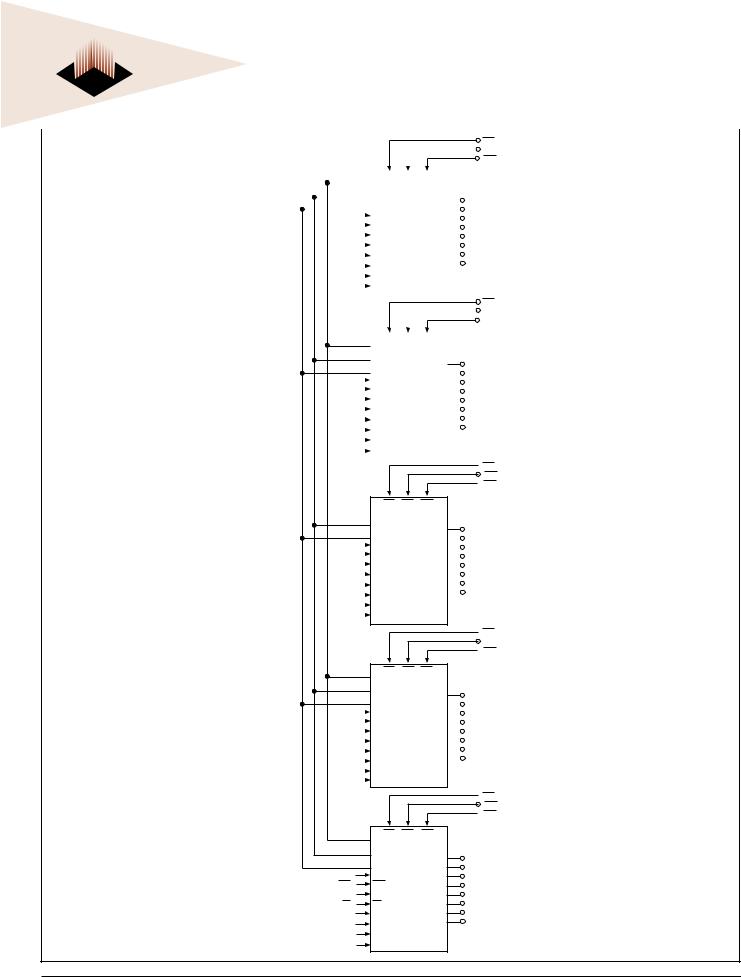
FIG. 2 FUNCTIONAL BLOCK DIAGRAM |
|
|
|
|
|
|
|
|
|
|
|
|
|
|
|
|
|
|
|
|
|
WE0 |
|
|||||||||||||
|
|
|
|
|
|
|
|
|
|
|
|
|
|
|
|
|
|
|
|
|
RAS0 |
|||||||||||||||
|
|
|
|
|
|
|
|
|
|
|
|
|
|
|
|
|
|
|
|
|
|
|
|
|
|
|
|
|
|
|
|
|
|
CAS0 |
||
|
|
|
|
|
|
|
|
|
|
|
|
|
|
|
|
|
|
|
|
|
|
|
|
|
|
|
|
|
|
|
|
|||||
|
|
|
|
|
|
|
|
|
|
|
|
|
|
|
|
|
|
|
|
|
|
|
|
|
|
|
|
|
|
|
|
|
|
|
|
|
VREF |
|
|
|
|
|
|
|
|
|
|
|
|
|
|
WE RAS CAS |
|
|
|
|
|
||||||||||||||||
|
VREF |
|
|
|
|
|
|
|
|
|
|
|
|
|
|
|
||||||||||||||||||||
A0-12 |
|
|
|
|
|
|
|
|
|
|
|
|
|
A0-12 |
|
|
|
|
|
DQ0 |
|
|
|
DQ0 |
||||||||||||
|
|
|
|
|
|
|
|
|
|
|
|
|
|
|
|
|
|
|
|
|
||||||||||||||||
BA0-1 |
|
|
|
|
|
|
|
|
|
|
|
|
|
BA0-1 |
|
|
|
|
|
|
|
|
||||||||||||||
|
|
|
|
|
|
|
|
|
|
|
|
|
|
|
|
|
|
|
|
=Y |
|
|
|
=Y |
||||||||||||
|
CLK0 |
|
|
|
|
|
CLK |
|
|
|
|
|
|
|
|
|||||||||||||||||||||
|
|
|
|
|
|
|
|
|
|
|
=Y |
|
|
|
=Y |
|||||||||||||||||||||
|
|
|
|
|
|
|
|
|
|
|
|
|||||||||||||||||||||||||
|
|
|
|
|
|
|
|
|
|
|
|
|
|
|
|
|
|
|
|
|
|
|
|
|
|
|
|
|
|
|
||||||
|
|
CLK0 |
|
|
|
|
|
|
|
CLK |
U0 |
|
|
|
=Y |
|
|
|
=Y |
|||||||||||||||||
|
|
|
|
|
|
|
|
|
|
|
||||||||||||||||||||||||||
|
|
CKE0 |
|
|
|
|
|
|
|
CKE |
|
|
|
|
|
|||||||||||||||||||||
|
|
|
|
|
|
|
|
|
|
|
|
|
|
|
|
=Y |
|
|
=Y |
|||||||||||||||||
|
|
|
|
|
|
|
|
|
|
|
|
|
||||||||||||||||||||||||
|
|
|
|
|
|
|
|
|
|
|
|
|
|
|
|
|
|
|
|
|
|
|
|
|
|
|
=Y |
|||||||||
|
|
|
CS0 |
|
|
|
|
|
|
|
CS |
|
|
|
|
|
|
|
=Y |
|
|
|
||||||||||||||
|
|
|
|
|
|
|
|
|
|
|
|
|
|
DQML |
|
|
|
|
|
|
|
=Y |
|
|
|
=Y |
||||||||||
|
|
|
|
|
|
|
|
|
|
|
|
|
|
|
|
|
|
|
||||||||||||||||||
|
|
DQML0 |
|
|
|
|
|
|
|
|
|
|||||||||||||||||||||||||
|
|
|
|
|
|
|
|
|
|
|
|
|
|
|
|
|
||||||||||||||||||||
|
|
DQMH0 |
|
|
|
|
|
|
|
DQMH |
|
|
|
|
|
DQ15 |
|
|
DQ15 |
|||||||||||||||||
|
|
|
|
|
|
|
|
|
|
|
|
|
|
|||||||||||||||||||||||
|
|
|
|
|
|
|
|
|
|
|
|
|
|
|
|
|
|
|
|
|
|
|
|
|||||||||||||
|
|
DQSL0 |
|
|
|
|
|
DQSL |
|
|
|
|
|
|
|
|
|
|
|
|
|
|
|
|||||||||||||
|
|
|
|
|
|
|
|
|
|
|
|
|
|
|
|
|
|
|
||||||||||||||||||
|
|
DQSH0 |
|
|
|
|
|
DQSH |
|
|
|
|
|
|
|
|
|
|
|
|
|
WE1 |
|
|||||||||||||
|
|
|
|
|
|
|
|
|
|
|
|
|
|
|
|
|
||||||||||||||||||||
|
|
|
|
|
|
|
|
|
|
|
|
|
|
|
|
|
|
|
|
|
|
|
|
|
|
|
|
|
|
|
|
|
|
|
||
|
|
|
|
|
|
|
|
|
|
|
|
|
|
|
|
|
|
|
|
|
|
|
|
|
|
|
|
|
|
|
|
|
|
|
||
|
|
|
|
|
|
|
|
|
|
|
|
|
|
|
|
|
|
|
|
|
|
|
|
|
|
|
|
|
|
|
|
|
|
|
RAS1 |
|
|
|
|
|
|
|
|
|
|
|
|
|
|
|
|
|
|
|
|
|
|
|
|
|
|
|
|
|
|
|
|
|
|
|
CAS1 |
||
|
|
|
|
|
|
|
|
|
|
|
|
|
|
|
|
|
|
|
|
|
|
|
|
|
|
|
|
|
|
|
||||||
|
|
|
|
|
|
|
|
|
|
|
|
|
|
|
|
|
|
|
|
|
|
|
|
|
|
|
|
|
|
|||||||
|
|
|
|
|
|
|
|
|
|
|
|
|
|
|
|
WE RAS CAS |
|
|
|
|
|
|
|
|||||||||||||
|
|
|
|
|
|
|
|
|
|
|
|
|
|
VREF |
|
|
|
|
|
|
|
|
|
|
|
|
|
|
|
|||||||
|
|
|
|
|
|
|
|
|
|
|
|
|
|
A0-12 |
|
|
|
|
|
DQ0 |
|
|
|
DQ16 |
||||||||||||
|
|
|
|
|
|
|
|
|
|
|
|
|
|
|
|
|
|
|
|
|
|
|
|
|
|
|
|
|||||||||
|
|
CLK1 |
|
|
|
|
|
|
|
|
BA0-1 |
|
|
|
|
|
|
|
=Y |
|
=Y |
|||||||||||||||
|
|
|
|
|
|
|
|
|
|
|
|
|
|
|
|
|
|
|
||||||||||||||||||
|
|
|
|
|
|
CLK |
|
|
|
|
|
|
|
=Y |
|
=Y |
||||||||||||||||||||
|
|
|
|
|
|
|
|
|
|
|
|
|
||||||||||||||||||||||||
|
|
CLK1 |
|
|
|
|
|
|
|
CLK |
U1 |
|
|
|
=Y |
|
|
|
=Y |
|||||||||||||||||
|
|
|
|
|
|
|
|
|
|
|
||||||||||||||||||||||||||
|
|
CKE1 |
|
|
|
|
|
|
|
CKE |
|
|
|
|
|
|
||||||||||||||||||||
|
|
|
|
|
|
|
|
|
|
|
|
|
|
|
|
=Y |
|
=Y |
||||||||||||||||||
|
|
|
|
|
|
|
|
|
|
|
|
|
|
|
||||||||||||||||||||||
|
|
|
|
|
|
|
|
|
|
|
|
|
|
|
|
|
|
|
|
|
|
|
|
=Y |
|
=Y |
||||||||||
|
|
|
CS1 |
|
|
|
|
|
|
|
CS |
|
|
|
|
|
|
|
|
|
|
|||||||||||||||
|
|
|
|
|
|
|
|
|
|
|
|
|
|
DQML |
|
|
|
|
|
|
|
=Y |
|
=Y |
||||||||||||
|
|
|
|
|
|
|
|
|
|
|
|
|
|
|
|
|
|
|
|
|
|
|
||||||||||||||
|
|
DQML1 |
|
|
|
|
|
|
|
|
|
|
||||||||||||||||||||||||
|
|
|
|
|
|
|
|
|
|
|
|
|
|
|
|
|
||||||||||||||||||||
|
|
DQMH1 |
|
|
|
|
|
|
|
DQMH |
|
|
|
|
|
DQ15 |
|
DQ31 |
||||||||||||||||||
|
|
|
|
|
|
|
|
|
|
|
|
|
|
|
|
|||||||||||||||||||||
|
|
|
|
|
|
|
|
|
|
|
|
|
|
|
|
|
|
|
|
|
|
|
|
|||||||||||||
|
|
DQSL1 |
|
|
|
|
|
DQSL |
|
|
|
|
|
|
|
|
|
|
|
|
|
|
|
|||||||||||||
|
|
|
|
|
|
|
|
|
|
|
|
|
|
|
|
|
|
|
||||||||||||||||||
|
|
DQSH1 |
|
|
|
|
|
DQSH |
|
|
|
|
|
|
|
|
|
|
|
|
|
|
|
|||||||||||||
|
|
|
|
|
|
|
|
|
|
|
|
|
|
|
|
|
|
|
||||||||||||||||||
|
|
|
|
|
|
|
|
|
|
|
|
|
|
|
|
|
|
|
|
|
|
|
|
|
|
|
|
|
|
|
|
|
|
|
|
|
 WE2
WE2
 RAS2
RAS2
 CAS2
CAS2
WE RAS CAS
 VREF
VREF
A0-12
DQ0 DQ32
|
|
|
|
|
|
|
|
BA0-1 |
|
=Y |
|
|
=Y |
||
|
|
|
|
|
|
|
|||||||||
CLK2 |
|
|
|
CLK |
|
=Y |
|
|
=Y |
||||||
|
|
|
|
|
|||||||||||
|
|
||||||||||||||
|
|
|
|
|
|
|
|
|
|
|
|
|
|||
CLK2 |
|
|
|
CLK |
U2 |
=Y |
|
|
=Y |
||||||
|
|
|
|||||||||||||
CKE2 |
|
|
|
CKE |
|
|
|||||||||
|
|
|
|
=Y |
|
|
=Y |
||||||||
|
|
|
|
||||||||||||
|
|
|
|
|
|
|
|
|
|
|
|
=Y |
|
|
=Y |
|
CS2 |
|
|
|
CS |
|
|
|
|||||||
DQML2 |
|
|
|
DQML |
|
=Y |
|
|
=Y |
||||||
|
|
|
|
|
|||||||||||
|
|
|
|
|
|
|
|
||||||||
DQMH2 |
|
|
|
DQMH |
|
DQ15 |
|
|
DQ47 |
||||||
|
|
|
|
|
|
||||||||||
|
|
|
|
|
|
|
|
||||||||
DQSL2 |
|
|
|
DQSL |
|
|
|
|
|
||||||
|
|
|
|
|
|
|
|||||||||
DQSH2 |
|
|
|
DQSH |
|
|
|
|
|
||||||
|
|
|
|
|
|
|
|||||||||
 WE3
WE3
 RAS3
RAS3
 CAS3
CAS3
WE RAS CAS
VREF
A0-12
DQ0 DQ48
|
|
|
|
|
|
|
BA0-1 |
|
=Y |
|
|
=Y |
|
|
|
|
|
|
|
|
|
||||||
CLK3 |
|
|
|
|
CLK |
|
=Y |
|
|
=Y |
|||
CLK3 |
|
|
|
CLK |
U3 |
=Y |
|
|
=Y |
||||
|
|
|
|||||||||||
CKE3 |
|
|
|
CKE |
|
=Y |
|
|
=Y |
||||
|
|
|
|
||||||||||
|
|
|
|
|
|
|
|
|
|
=Y |
|
|
=Y |
CS3 |
|
|
|
CS |
|
|
|
||||||
|
|
|
|
||||||||||
DQML3 |
|
|
|
DQML |
|
=Y |
|
|
=Y |
||||
|
|
|
|
|
|
||||||||
|
|
|
|
|
|
|
|
||||||
DQMH3 |
|
|
|
DQMH |
|
DQ15 |
|
|
DQ63 |
||||
|
|
|
|
|
|
||||||||
|
|
|
|
|
|
|
|
||||||
DQSL3 |
|
|
|
DQSL |
|
|
|
|
|
||||
|
|
|
|
|
|
||||||||
DQSH3 |
|
|
|
DQSH |
|
|
|
|
|
||||
|
|
|
|
|
|
||||||||
 WE4
WE4
 RAS4
RAS4
 CAS4
CAS4
|
WE |
RAS CAS |
|
|
|
VREF |
|
|
|
|
A0-12 |
|
DQ0 |
DQ64 |
|
|
|
||
|
BA0-1 |
|
=Y |
=Y |
CLK4 |
CLK |
|
=Y |
=Y |
CLK4 |
CLK |
U4 |
=Y |
=Y |
CKE4 |
CKE |
|
=Y |
=Y |
CS4 |
CS |
|
=Y |
=Y |
DQML4 |
DQML |
|
=Y |
=Y |
|
|
|
||
DQMH4 |
DQMH |
|
DQ15 |
DQ79 |
|
|
|
||
DQSL4 |
DQSL |
|
|
|
DQSH4 |
DQSH |
|
|
|
|
3 |
|
White Electronic Designs Corporation • (602) 437-1520 • www.whiteedc.com |
|

White Electronic Designs |
WEDPND16M72S-XBX |
strobe transmitted by the DDR SDRAM during READs and by the memory contoller during WRITEs. DQS is edge-aligned with data for READs and center-aligned with data for WRITEs. Each chip has two data strobes, one for the lower byte and one for the upper byte.
The 128MB DDR SDRAM operates from a differential clock (CLK and CLK); the crossing of CLK going HIGH and CLK going LOW will be referred to as the positive edge of CLK. Commands (address and control signals) are registered at every positive edge of CLK. Input data is registered on both edges of DQS, and output data is referenced to both edges of DQS, as well as to both edges of CLK.
Read and write accesses to the DDR SDRAM are burst oriented; accesses start at a selected location and continue for a programmed number of locations in a programmed sequence. Accesses begin with the registration of an ACTIVE command, which is then followed by a READ or WRITE command. The address bits registered coincident with the ACTIVE command are used to select the bank and row to be accessed. The address bits registered coincident with the READ or WRITE command are used to select the bank and the starting column location for the burst access.
The DDR SDRAM provides for programmable READ or WRITE burst lengths of 2, 4, or 8 locations. An auto precharge function may be enabled to provide a self-timed row precharge that is initiated at the end of the burst access.
The pipelined, multibank architecture of DDR SDRAMs allows for concurrent operation, thereby providing high effective bandwidth by hiding row precharge and activation time.
An auto refresh mode is provided, along with a powersaving power-down mode.
FUNCTIONAL DESCRIPTION
Read and write accesses to the DDR SDRAM are burst oriented; accesses start at a selected location and continue for a programmed number of locations in a programmed sequence. Accesses begin with the registration of an ACTIVE command which is then followed by a READ or WRITE command. The address bits registered coincident with the ACTIVE command are used to select the bank and row to be accessed (BA0 and BA1 select the bank, A0-12 select the row). The address bits registered coincident with the READ or WRITE command are used to select the starting column location for the burst access.
Prior to normal operation, the SDRAM must be initialized. The following sections provide detailed information cover-
ing device initialization, register definition, command descriptions and device operation.
INITIALIZATION
DDR SDRAMs must be powered up and initialized in a predefined manner. Operational procedures other than those specified may result in undefined operation. Power must first be applied to VCC and VCCQ simultaneously, and then to VREF (and to the system VTT). VTT must be applied after VCCQ to avoid device latch-up, which may cause permanent damage to the device. VREF can be applied any time after VCCQ but is expected to be nominally coincident with VTT. Except for CKE, inputs are not recognized as valid until after VREF is applied. CKE is an SSTL_2 input but will detect an LVCMOS LOW level after VCC is applied. Maintaining an LVCMOS LOW level on CKE during power-up is required to ensure that the DQ and DQS outputs will be in the High-Z state, where they will remain until driven in normal operation (by a read access). After all power supply and reference voltages are stable, and the clock is stable, the DDR SDRAM requires a 200ms delay prior to applying an executable command.
Once the 200ms delay has been satisfied, a DESELECT or NOP command should be applied, and CKE should be brought HIGH. Following the NOP command, a PRECHARGE ALL command should be applied. Next a LOAD MODE REGISTER command should be issued for the extended mode register (BA1 LOW and BA0 HIGH) to enable the DLL, followed by another LOAD MODE REGISTER command to the mode register (BA0/BA1 both LOW) to reset the DLL and to program the operating parameters. Two-hundred clock cycles are required between the DLL reset and any READ command. A PRECHARGE ALL command should then be applied, placing the device in the all banks idle state.
Once in the idle state, two AUTO REFRESH cycles must be performed (tRFC must be satisfied.) Additionally, a LOAD MODE REGISTER command for the mode register with the reset DLL bit deactivated (i.e., to program operating parameters without resetting the DLL) is required. Following these requirements, the DDR SDRAM is ready for normal operation.
REGISTER DEFINITION
MODE REGISTER
The Mode Register is used to define the specific mode of operation of the DDR SDRAM. This definition includes the
White Electronic Designs Corporation • Phoenix AZ • (602) 437-1520 |
4 |

 White Electronic Designs WEDPND16M72S-XBX
selection of a burst length, a burst type, a CAS latency, and an operating mode, as shown in Figure 3. The Mode Register is programmed via the MODE REGISTER SET command (with BA0 = 0 and BA1 = 0) and will retain the stored information until it is programmed again or the device loses power. (Except for bit A8 which is self clearing).
Reprogramming the mode register will not alter the contents of the memory, provided it is performed correctly. The Mode Register must be loaded (reloaded) when all banks are idle and no bursts are in progress, and the controller must wait the specified time before initiating the subsequent operation. Violating either of these requirements will result in unspecified operation.
Mode register bits A0-A2 specify the burst length, A3 specifies the type of burst (sequential or interleaved), A4-A6 specify the CAS latency, and A7-A12 specify the operating mode.
BURST TYPE
Accesses within a given burst may be programmed to be either sequential or interleaved; this is referred to as the burst type and is selected via bit M3.
The ordering of accesses within a burst is determined by the burst length, the burst type and the starting column address, as shown in Table 1.
READ LATENCY
The READ latency is the delay, in clock cycles, between the registration of a READ command and the availability of the first bit of output data. The latency can be set to 2 or 2.5 clocks.
If a READ command is registered at clock edge n, and the latency is m clocks, the data will be available by clock edge n+m. Table 2 below indicates the operating frequencies at which each CAS latency setting can be used.
BURST LENGTH
Read and write accesses to the DDR SDRAM are burst oriented, with the burst length being programmable, as shown in Figure 3. The burst length determines the maximum number of column locations that can be accessed for a given READ or WRITE command. Burst lengths of 2, 4 or 8 locations are available for both the sequential and the interleaved burst types.
Reserved states should not be used, as unknown operation or incompatibility with future versions may result.
When a READ or WRITE command is issued, a block of columns equal to the burst length is effectively selected. All accesses for that burst take place within this block, meaning that the burst will wrap within the block if a boundary is reached. The block is uniquely selected by A1-Ai when the burst length is set to two; by A2-Ai when the burst length is set to four (where Ai is the most significant column address for a given configuration); and by A3-Ai when the burst length is set to eight. The remaining (least significant) address bit(s) is (are) used to select the starting location within the block. The programmed burst length applies to both READ and WRITE bursts.
Reserved states should not be used as unknown operation or incompatibility with future versions may result.
TABLE 2 - CAS LATENCY
|
ALLOWABLE OPERATING |
|
|
FREQUENCY (MHz) |
|
|
|
|
|
CAS |
CAS |
SPEED |
LATENCY = 2 |
LATENCY = 2.5 |
-200 |
£ 75 |
£ 100 |
-250 |
£ 100 |
£ 125 |
-266 |
£ 100 |
£ 133 |
OPERATING MODE
The normal operating mode is selected by issuing a MODE REGISTER SET command with bits A7-A12 each set to zero, and bits A0-A6 set to the desired values. A DLL reset is initiated by issuing a MODE REGISTER SET command with bits A7 and A9-A12 each set to zero, bit A8 set to one, and bits A0-A6 set to the desired values. Although not required, JEDEC specifications recommend when a LOAD MODE REGISTER command is issued to reset the DLL, it should always be followed by a LOAD MODE REGISTER command to select normal operating mode.
All other combinations of values for A7-A12 are reserved for future use and/or test modes. Test modes and reserved states should not be used because unknown operation or incompatibility with future versions may result.
5White Electronic Designs Corporation • (602) 437-1520 • www.whiteedc.com
 Loading...