


WMS128K8L-85FEMA
White Electronic Designs WMS128K8L-85FEMA, WMS128K8L-85FEM, WMS128K8L-85FEIA, WMS128K8L-85FEI, WMS128K8L-85FECA Datasheet
...
11
11
1 White Electronic Designs Corporation • (602) 437-1520 • www.whiteedc.com
White Electronic Designs
WMS128K8-XXX
n MIL-STD-883 Compliant Devices Available
n Commercial, Industrial and Military Temperature Range
n 5 Volt Power Supply
n Low Power CMOS
n 2V Data Retention Devices Available
(Low Power Version)
n TTL Compatible Inputs and Outputs
128Kx8 MONOLITHIC SRAM, SMD 5962-96691
FEATURES
n Access Times 70, 85, 100, 120ns
n Revolutionary, Center Power/Ground Pinout
JEDEC Approved
• 32 lead Ceramic SOJ (Package 101)
n Evolutionary, Corner Power/Ground Pinout
JEDEC Approved
• 32 pin Ceramic DIP (Package 300)
• 32 lead Ceramic SOJ (Package 101)
• 32 lead Ceramic Flat Pack (Package 206)
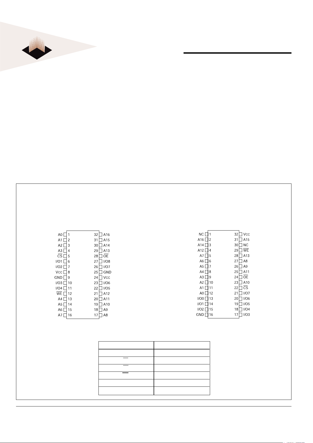
EVOLUTIONARY PINOUT
REVOLUTIONARY PINOUT
A0-16 Address Inputs
I/O0-7 Data Input/Output
CS Chip Select
OE Output Enable
WE Write Enable
VCC +5.0V Power
GND Ground
PIN DESCRIPTION
3232
3232
32
DIP (C)DIP (C)
DIP (C)DIP (C)
DIP (C)
3232
3232
32
CC
CC
C
SOJ (DE)SOJ (DE)
SOJ (DE)SOJ (DE)
SOJ (DE)
32 FL32 FL
32 FL32 FL
32 FL
AA
AA
A
TPTP
TPTP
TP
AA
AA
A
CK (FE)CK (FE)
CK (FE)CK (FE)
CK (FE)
TOP VIEW
32 C32 C
32 C32 C
32 C
SOJ (DR)SOJ (DR)
SOJ (DR)SOJ (DR)
SOJ (DR)
SEPTEMBER 2002 REV. 5
TOP VIEW

22
22
2
White Electronic Designs Corporation • Phoenix AZ • (602) 437-1520
White Electronic Designs
WMS128K8-XXX
ParameterParameter
ParameterParameter
Parameter
SymSym
SymSym
Sym
ConditionsConditions
ConditionsConditions
Conditions
-70-70
-70-70
-70
-85-85
-85-85
-85
-100-100
-100-100
-100
-120-120
-120-120
-120
UnitsUnits
UnitsUnits
Units
MinMin
MinMin
Min
MaxMax
MaxMax
Max
MinMin
MinMin
Min
MaxMax
MaxMax
Max
MinMin
MinMin
Min
MaxMax
MaxMax
Max
MinMin
MinMin
Min
MaxMax
MaxMax
Max
Input Leakage Current ILI VCC = 5.5, VIN = GND to VCC 10 10 10 10 µA
Output Leakage Current I LO CS = VIH, OE = VIH, VOUT = GND to VCC 10 10 10 10 µA
Operating Supply Current ICC CS = VIL, OE = VIH, f = 5MHz, Vcc = 5.5 30 30 30 30 mA
Standby Current ISB CS = VIH, OE = VIH, f = 5MHz, Vcc = 5.5 5 5 5 5 mA
Output Low Voltage VOL IOL = 2.1mA, Vcc = 4.5 0.4 0.4 0.4 0.4 V
Output High Voltage V
OH IOH = -1.0mA, Vcc = 4.5 2.4 2.4 2.4 2.4 V
ABSOLUTE MAXIMUM RATINGS
TRUTH TABLE
RECOMMENDED OPERATING CONDITIONS
PP
PP
P
arameterarameter
arameterarameter
arameter
Symbol Symbol
Symbol Symbol
Symbol
MinMin
MinMin
Min
MaxMax
MaxMax
Max
UnitUnit
UnitUnit
Unit
Operating Temperature T
A -55 +125 °C
Storage Temperature T
STG -65 +150 °C
Signal Voltage Relative to GND V
G -0.5 Vcc+0.5 V
Junction Temperature T
J 150 °C
Supply Voltage V
CC -0.5 7.0 V
PP
PP
P
arameterarameter
arameterarameter
arameter
SymbolSymbol
SymbolSymbol
Symbol
MinMin
MinMin
Min
MaxMax
MaxMax
Max
UnitUnit
UnitUnit
Unit
Supply Voltage V
CC 4.5 5.5 V
Input High Voltage V
IH 2.2 VCC + 0.3 V
Input Low Voltage V
IL -0.5 +0.8 V
DC CHARACTERISTICS
(VCC
= 5.0V, GND = 0V, TA = -55°C TO +125°C)
DATA RETENTION CHARACTERISTICS
(TA
= -55°C TO +125°C)
CC
CC
C
SS
SS
S
OEOE
OEOE
OE
WEWE
WEWE
WE
ModeMode
ModeMode
Mode
Data I/OData I/O
Data I/OData I/O
Data I/O
P P
P P
P
owerower
owerower
ower
H X X Standby High Z Standby
L L H Read Data Out Active
L H H Out Disable High Z Active
L X L Write Data In Active
ParameterParameter
ParameterParameter
Parameter
SymbolSymbol
SymbolSymbol
Symbol
ConditionsConditions
ConditionsConditions
Conditions
-70-70
-70-70
-70
-85-85
-85-85
-85
-100-100
-100-100
-100
-120-120
-120-120
-120
UnitsUnits
UnitsUnits
Units
MinMin
MinMin
Min
MaxMax
MaxMax
Max
MinMin
MinMin
Min
MaxMax
MaxMax
Max
MinMin
MinMin
Min
MaxMax
MaxMax
Max
MinMin
MinMin
Min
MaxMax
MaxMax
Max
Data Retention
Supply Voltage V DR CS ≥ V CC -0.2V 2.0 5.5 2.0 5.5 2.0 5.5 2.0 5.5 V
Data Retention
Current I
CCDR1 VCC = 3V 1 1 1 1
mA
CAPACITANCE
(TA = +25°C)
ParameterParameter
ParameterParameter
Parameter
SymbolSymbol
SymbolSymbol
Symbol
ConditionCondition
ConditionCondition
Condition
PackagePackage
PackagePackage
Package
MaxMax
MaxMax
Max
UnitUnit
UnitUnit
Unit
Input capacitance C
IN
V
IN
= 0V, f = 1.0MHz
32 Pin CSOJ, DIP, 12 pF
Flat Pack Evolutionary
32 Pin CSOJ Revolutionary 20 pF
Output capicitance C
OUT
V
OUT
= 0V, f = 1.0MHz
32 Pin CSOJ, DIP, 12 pF
Flat Pack Evolutionary
32 Pin CSOJ Revolutionary 20 pF
This parameter is guaranteed by design but not tested.
NOTE: DC test conditions: VIH = VCC -0.3V, VIL = 0.3V

33
33
3 White Electronic Designs Corporation • (602) 437-1520 • www.whiteedc.com
White Electronic Designs
WMS128K8-XXX
Notes:
VZ is programmable from -2V to +7V.
IOL & IOH programmable from 0 to 16mA.
Tester Impedance Z0 = 75Ω.
VZ is typically the midpoint of VOH and VOL.
IOL & IOH
are adjusted to simulate a typical resistive load circuit.
ATE tester includes jig capacitance.
AC TEST CIRCUIT
AC TEST CONDITIONS
ParameterParameter
ParameterParameter
Parameter
TypTyp
TypTyp
Typ
UnitUnit
UnitUnit
Unit
Input Pulse Levels VIL = 0, VIH = 3.0 V
Input Rise and Fall 5 ns
Input and Output Reference Level 1. 5 V
Output Timing Reference Level 1.5 V
ParameterParameter
ParameterParameter
Parameter
SymbolSymbol
SymbolSymbol
Symbol
-70-70
-70-70
-70
-85-85
-85-85
-85
-100-100
-100-100
-100
-120-120
-120-120
-120
UnitsUnits
UnitsUnits
Units
Read CycleRead Cycle
Read CycleRead Cycle
Read Cycle
MinMin
MinMin
Min
MaxMax
MaxMax
Max
MinMin
MinMin
Min
MaxMax
MaxMax
Max
MinMin
MinMin
Min
MaxMax
MaxMax
Max
MinMin
MinMin
Min
MaxMax
MaxMax
Max
Read Cycle Time t
RC 70 85 100 120 ns
Address Access Time t
AA 70 85 100 120 ns
Output Hold from Address Change t
OH 3333ns
Chip Select Access Time t
ACS 70 85 100 120 ns
Output Enable to Output Valid t
OE 35 45 50 60 ns
Chip Select to Output in Low Z t
CLZ
1
3333ns
Output Enable to Output in Low Z t
OLZ
1
0000ns
Chip Disable to Output in High Z t
CHZ
1
25 25 35 35 ns
Output Disable to Output in High Z tOHZ
1
25 25 35 35 ns
AC CHARACTERISTICS
(VCC
= 5.0V, TA
= -55°C TO +125°C)
AC CHARACTERISTICS
(VCC
= 5.0V, TA
= -55°C TO +125°C)
ParameterParameter
ParameterParameter
Parameter
SymbolSymbol
SymbolSymbol
Symbol
-70-70
-70-70
-70
-85-85
-85-85
-85
-100-100
-100-100
-100
-120-120
-120-120
-120
UnitsUnits
UnitsUnits
Units
Write CycleWrite Cycle
Write CycleWrite Cycle
Write Cycle
MinMin
MinMin
Min
MaxMax
MaxMax
Max
MinMin
MinMin
Min
MaxMax
MaxMax
Max
MinMin
MinMin
Min
MaxMax
MaxMax
Max
MinMin
MinMin
Min
MaxMax
MaxMax
Max
Write Cycle Time t
WC 70 85 100 120 ns
Chip Select to End of Write t
CW 60 75 80 100 ns
Address Valid to End of Write t
AW 60 75 80 100 ns
Data Valid to End of Write t
DW 30 35 40 50 ns
Write Pulse Width t
WP 50 55 70 80 ns
Address Setup Time t
AS 0000ns
Address Hold Time t
AH 5555ns
Output Active from End of Write t
OW
1
5555ns
Write Enable to Output in High Z t
WHZ
1
25 30 35 35 ns
Data Hold Time t
DH 0000ns
1. This parameter is guaranteed by design but not tested.
1. This parameter is guaranteed by design but not tested.
 Loading...