


White Electronic Designs WSE128K16-73H1MA, WSE128K16-73H1M, WSE128K16-73H1IA, WSE128K16-73H1I, WSE128K16-73H1CA Datasheet
...128KX16 SRAM/EEPROM MODULE
FEATURES
■Access Times of 35ns (SRAM) and 150ns (EEPROM)
■Access Times of 45ns (SRAM) and 120ns (EEPROM)
■Access Times of 70ns (SRAM) and 300ns (EEPROM)
■Packaging
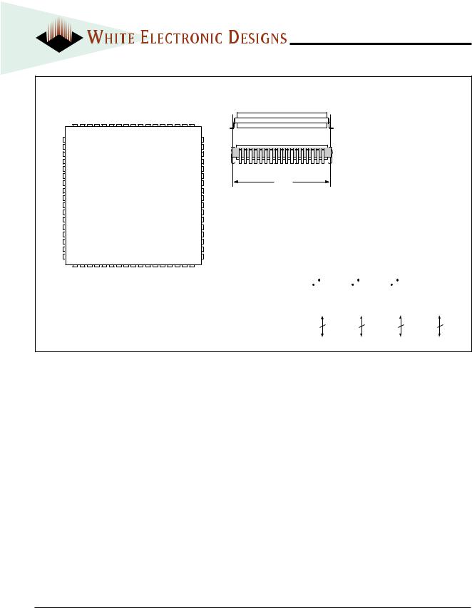
•66 pin, PGA Type, 1.075" square HIP, Hermetic Ceramic HIP (H1) (Package 400)
•68 lead, Hermetic CQFP (G2T), 22mm (0.880") square (Package 509). Designed to fit JEDEC 68 lead 0.990" CQFJ footprint (Fig. 2)
■128Kx16 SRAM
■128Kx16 EEPROM
■Organized as 128Kx16 of SRAM and 128Kx16 of EEPROM Memory with separate Data Buses
■Both blocks of memory are User Configurable as 256Kx8
■Low Power CMOS
■Commercial, Industrial and Military Temperature Ranges
WSE128K16-XXX
PRELIMINARY*
■TTL Compatible Inputs and Outputs
■Built-in Decoupling Caps and Multiple Ground Pins for Low Noise Operation
■Weight - 13 grams typical
EEPROM MEMORY FEATURES
■Write Endurance 10,000 Cycles
■Data Retention at 25°C, 10 Years
■Low Power CMOS Operation
■Automatic Page Write Operation
■Page Write Cycle Time 10ms Max.
■Data Polling for End of Write Detection
■Hardware and Software Data Protection
■TTL Compatible Inputs and Outputs
*This data sheet describes a product under development, not fully characterized, and is subject to change without notice.
FIG.1 |
PIN CONFIGURATION FOR WSE128K16-XH1X |
|
|
|
|
|
|
|
|
|
|
|
|
|
|
|
|
|
|
|
|
PIN DESCRIPTION |
|||||||||||||||||||||||||||||||
|
|
|
|
|
|
|
|
|
|
|
|
|
|
|
|
|
|
|
|
|
|
|
|
|
|
|
|
|
|
|
|
|
|
|
|
|
|
||||||||||||||||
|
|
|
TOP VIEW |
|
|
|
|
|
|
|
|
|
|
|
|
|
|
|
|
|
|
|
|
|
|
|
|
|
|
|
|
|
|
|
|
|
|
|
|
||||||||||||||
|
|
|
|
|
|
|
|
|
|
|
|
|
|
|
|
|
|
|
|
|
|
|
|
|
|
|
|
|
|
ED0-15 |
|
EEPROM Data Inputs/Outputs |
|
||||||||||||||||||||
1 |
12 |
23 |
|
34 |
45 |
|
56 |
|
|
|
|
|
|
|
|
|
|
|
|
|
|
|
|
|
|
|
|
|
|
|
SD0-15 |
|
SRAM Data Inputs/Outputs |
|
|||||||||||||||||||
|
|
|
|
|
|
|
|
|
|
|
|
|
|
|
|
|
|
|
|
|
|
|
|
|
|
|
|
|
|
|
|
|
|
||||||||||||||||||||
|
SD8 |
SWE2 |
SD15 |
ED8 |
|
VCC |
ED15 |
|
|
|
|
|
|
|
|
|
|
|
|
|
|
|
|
|
|
|
|
|
|
|
|
A0-16 |
|
|
|
|
|
Address Inputs |
|
||||||||||||||
|
|
|
|
|
|
|
|
|
|
|
|
|
|
|
|
|
|
|
|
|
|
|
|
|
|
|
|
|
|
|
|
1-2 |
|
|
|
|
SRAM Write Enable |
|
|||||||||||||||
|
SD9 |
SCS2 |
SD14 |
ED9 |
|
ECS2 |
ED14 |
|
|
|
|
|
|
|
|
|
|
|
|
|
|
|
|
|
|
|
|
|
|
SWE |
|
|
|
|
|
||||||||||||||||||
|
|
|
|
|
|
|
|
|
|
|
|
|
|
|
|
|
|
|
|
|
|
|
|
|
|
|
|
|
|
|
|
|
|
|
|
1-2 |
|
|
|
|
SRAM Chip Selects |
|
|||||||||||
|
SD10 |
GND |
SD13 |
ED10 |
|
EWE2 |
ED13 |
|
|
|
|
|
|
|
|
|
|
|
|
|
|
|
|
|
|
|
|
|
|
SCS |
|
|
|
|
|
||||||||||||||||||
|
|
|
|
|
|
|
|
|
|
|
|
|
|
|
|
|
|
|
|
|
|
|
|
|
|
|
|
|
|
|
|
|
|
|
|
|
|
|
Output Enable |
|
|||||||||||||
|
|
|
|
|
|
|
|
|
|
|
|
|
|
|
|
|
|
|
|
|
|
|
|
|
|
|
|
|
|
|
|
|
OE |
|
|
|
|
|
|
|
|||||||||||||
|
A13 |
SD11 |
SD12 |
A6 |
|
ED11 |
ED12 |
|
|
|
|
|
|
|
|
|
|
|
|
|
|
|
|
|
|
|
|
|
|
|
|
VCC |
|
|
|
|
|
|
Power Supply |
|
|||||||||||||
|
|
|
|
|
|
|
|
|
|
|
|
|
|
|
|
|
|
|
|
|
|
|
|
|
|
|
|
|
|
|
|
|
|
|
|
|
|
|
|||||||||||||||
|
A14 |
A10 |
OE |
A7 |
|
A3 |
A0 |
|
|
|
|
|
|
|
|
|
|
|
|
|
|
|
|
|
|
|
|
|
|
|
|
GND |
|
|
|
|
|
|
|
|
Ground |
|
|||||||||||
|
|
|
|
|
|
|
|
|
|
|
|
|
|
|
|
|
|
|
|
|
|
|
|
|
|
|
|
|
|
|
|
|
|
|
|
|
|
|
|
|
|||||||||||||
|
A15 |
A11 |
NC |
NC |
|
A4 |
A1 |
|
|
|
|
|
|
|
|
|
|
|
|
|
|
|
|
|
|
|
|
|
|
|
|
|
NC |
|
|
|
|
|
Not Connected |
|
|||||||||||||
|
|
|
|
|
|
|
|
|
|
|
|
|
|
|
|
|
|
|
|
|
|
|
|
|
|
|
|
|
|
|
|
1-2 |
|
|
|
|
EEPROM Write Enable |
|
|||||||||||||||
|
A16 |
A12 |
SWE1 |
A8 |
|
A5 |
A2 |
|
|
|
|
|
|
|
|
|
|
|
|
|
|
|
|
|
|
|
|
|
|
EWE |
|
|
|
|
|
||||||||||||||||||
|
|
|
|
|
|
|
|
|
|
|
|
|
|
|
|
|
|
|
|
|
|
|
|
|
|
|
|
|
|
1-2 |
|
|
|
|
EEPROM Chip Select |
|
|||||||||||||||||
|
|
|
|
|
|
|
|
|
|
|
|
|
|
|
|
|
|
|
|
|
|
|
|
|
|
|
|
|
|
|
|
|
|
|
|
|
|||||||||||||||||
|
NC |
VCC |
SD7 |
A9 |
|
EWE1 |
ED7 |
|
|
|
|
|
|
|
|
|
|
|
|
|
|
|
|
|
|
|
|
|
|
|
ECS |
|
|
|
|
|
|||||||||||||||||
|
|
|
|
|
|
|
|
|
|
|
|
|
|
BLOCK DIAGRAM |
|
|
|
|
|
|
|
|
|
|
|||||||||||||||||||||||||||||
|
SD0 |
SCS1 |
SD6 |
ED0 |
|
ECS1 |
ED6 |
|
|
|
|
|
|
|
|
|
|
|
|
|
|
|
|
|
|
|
|
|
|
||||||||||||||||||||||||
|
|
|
|
|
|
|
|
|
|
|
|
|
|
|
|
|
|
|
|
|
|
|
|
|
|
|
|
|
|
|
|
|
|
|
|
|
|
|
|
|
|
|
|
|
|
|
|
||||||
|
|
|
|
|
|
|
|
|
|
|
|
|
|
|
|
|
|
|
|
|
|
|
|
|
|
|
|
|
|
|
|
|
|
|
|
|
|
|
|
|
|
|
|
||||||||||
|
|
|
|
|
|
|
|
|
|
|
|
|
|
SWE1 SCS1 SWE |
2 SCS2 |
|
|
|
|
EWE |
1 |
ECS1 |
|
|
EWE |
2 |
ECS2 |
||||||||||||||||||||||||||
|
|
|
|
|
|
|
|
|
|
|
|
|
|
|
|
|
|
|
|
|
|
|
|
|
|
|
|
|
|
|
|
|
|
|
|
|
|
|
|
|
|
|
|
|
|
|
|
|
|
|
|
|
|
|
SD1 |
NC |
SD5 |
ED1 |
|
GND |
ED5 |
|
OE |
|
|
|
|
|
|
|
|
|
|
|
|
|
|
|
|
|
|
|
|
|
|
|
|
|
|
|
|
|
|
|
|
|
|
|
|
|
|
|
|
|
|
||
|
SD2 |
SD3 |
SD4 |
ED2 |
|
ED3 |
ED4 |
|
A 0 - 1 6 |
|
|
|
|
|
|
|
|
|
|
|
|
|
|
|
|
|
|
|
|
|
|
|
|
|
|
|
|
|
|
|
|
|
|
|
|
|
|
|
|
|
|||
|
|
|
|
|
|
|
128K x 8 |
|
|
|
128K x 8 |
|
|
|
|
|
|
128K x 8 |
|
|
|
|
128K x 8 |
|
|
|
|||||||||||||||||||||||||||
|
|
|
|
|
|
|
|
|
|
|
|
|
|
|
|
|
|
|
|
|
|
|
|
|
|
|
|
|
|||||||||||||||||||||||||
|
|
|
|
|
|
|
|
|
|
|
|
|
|
SRAM |
|
|
|
|
SRAM |
|
|
|
|
|
|
EEPROM |
|
|
|
EEPROM |
|
|
|
||||||||||||||||||||
11 |
22 |
33 |
|
44 |
55 |
|
66 |
|
|
|
|
|
|
|
|
|
|
|
|
|
|
|
|
|
|
|
|
|
|||||||||||||||||||||||||
|
|
|
|
|
|
|
|
|
|
|
|
|
|
|
|
|
|
|
|
|
|
|
|
|
|
|
|
|
|
|
|
|
|
|
|
|
|
|
|
|
|
|
|
|
|
|
|||||||
|
|
|
|
|
|
|
|
|
|
|
|
|
|
|
|
|
|
|
|
|
|
|
|
|
|
|
|
|
|
|
|
|
|
|
|
|
|
|
|
|
|
|
|
|
|
|
|
|
|
|
|
|
|
|
|
|
|
|
|
|
|
8 |
|
8 |
|
|
|
|
|
8 |
|
|
|
|
8 |
|
|
|
|
|
|||||||||||||||||||||||||||
|
|
|
|
|
|
|
|
|
|
|
|
|
|
SD 0 - 7 |
|
|
|
|
SD 8 - 1 5 |
|
|
|
|
|
ED 0 - 7 |
|
|
|
|
|
ED 8 - 1 5 |
||||||||||||||||||||||
|
|
|
|
|
|
|
|
|
|
|
|
|
|
|
|
|
|
|
|
|
|
|
|
|
|
|
|
|
|
|
|
|
|
|
|
|
|
|
|
|
|
|
|
|
|
|
|
|
|
|
|
||
|
|
|
|
|
|
|
|
|
|
|
|
|
|
|
|
|
|
|
|
|
|
|
|
|
|
|
|
|
|
|
|
|
|
|
|
|
|
|
|
|
|
|
|
|
|
|
|
|
|
|
|
|
|
May 2001, Rev. 4 |
|
|
|
|
|
|
1 |
|
|
|
|
|
|
|
|
White Electronic Designs Corporation • (602) 437-1520 • www.whiteedc.com |
|||||||||||||||||||||||||||||||||||||
WSE128K16-XXX
FIG. 2 PIN CONFIGURATION FOR WSE128K16-XG2TX |
PIN DESCRIPTION |
|
TOP VIEW |
||
|
|
NC |
A0 |
A1 |
A2 |
A3 |
A4 |
A5 |
|
|
ECS1 |
|
GND |
|
ECS2 |
|
SWE1 |
|
A6 |
|
A7 |
|
A8 |
A9 |
A10 |
VCC |
|
|
|
|
|
|
|
|
|
|
||||||||||||||||||
|
|
|
|
|
|
|
||||||||||||||||||||
|
9 |
8 |
7 |
6 |
5 |
4 |
3 |
2 |
1 |
68 67 66 65 64 63 62 61 |
|
|||||||||||||||
SD0 |
10 |
|
|
|
|
|
|
|
|
|
|
|
|
|
|
|
|
|
|
|
|
|
|
|
60 |
ED0 |
SD1 |
11 |
|
|
|
|
|
|
|
|
|
|
|
|
|
|
|
|
|
|
|
|
|
|
|
59 |
ED1 |
SD2 |
12 |
|
|
|
|
|
|
|
|
|
|
|
|
|
|
|
|
|
|
|
|
|
|
|
58 |
ED2 |
SD3 |
13 |
|
|
|
|
|
|
|
|
|
|
|
|
|
|
|
|
|
|
|
|
|
|
|
57 |
ED3 |
SD4 |
14 |
|
|
|
|
|
|
|
|
|
|
|
|
|
|
|
|
|
|
|
|
|
|
|
56 |
ED4 |
SD5 |
15 |
|
|
|
|
|
|
|
|
|
|
|
|
|
|
|
|
|
|
|
|
|
|
|
55 |
ED5 |
SD6 |
16 |
|
|
|
|
|
|
|
|
|
|
|
|
|
|
|
|
|
|
|
|
|
|
|
54 |
ED6 |
SD7 |
17 |
|
|
|
|
|
|
|
|
|
|
|
|
|
|
|
|
|
|
|
|
|
|
|
53 |
ED7 |
GND |
18 |
|
|
|
|
|
|
|
|
|
|
|
|
|
|
|
|
|
|
|
|
|
|
|
52 |
GND |
SD8 |
19 |
|
|
|
|
|
|
|
|
|
|
|
|
|
|
|
|
|
|
|
|
|
|
|
51 |
ED8 |
SD9 |
20 |
|
|
|
|
|
|
|
|
|
|
|
|
|
|
|
|
|
|
|
|
|
|
|
50 |
ED9 |
SD10 |
21 |
|
|
|
|
|
|
|
|
|
|
|
|
|
|
|
|
|
|
|
|
|
|
|
49 |
ED10 |
SD11 |
22 |
|
|
|
|
|
|
|
|
|
|
|
|
|
|
|
|
|
|
|
|
|
|
|
48 |
ED11 |
SD12 |
23 |
|
|
|
|
|
|
|
|
|
|
|
|
|
|
|
|
|
|
|
|
|
|
|
47 |
ED12 |
SD13 |
24 |
|
|
|
|
|
|
|
|
|
|
|
|
|
|
|
|
|
|
|
|
|
|
|
46 |
ED13 |
SD14 |
25 |
|
|
|
|
|
|
|
|
|
|
|
|
|
|
|
|
|
|
|
|
|
|
|
45 |
ED14 |
SD15 |
26 |
|
|
|
|
|
|
|
|
|
|
|
|
|
|
|
|
|
|
|
|
|
|
|
44 |
ED15 |
|
27 28 29 30 31 32 33 34 35 36 37 38 39 40 41 42 43 |
|
||||||||||||||||||||||||
|
VCC |
A11 |
A12 |
A13 |
A14 |
A15 |
A16 |
|
|
SCS1 |
|
OE |
|
SCS2 |
|
NC |
|
SWE2 |
|
EWE1 |
|
EWE2 |
NC |
NC |
NC |
|
|
|
|
|
|
|
|
|
|
|
|||||||||||||||||
|
|
|
|
|
|
|||||||||||||||||||||
|
|
|
|
|
|
|
|
|
|
|
|
|
|
|
|
|
|
|
|
|
|
|
|
|||
0.940"
The WEDC 68 lead G2T CQFP fills the same fit and function as the JEDEC 68 lead CQFJ or 68 PLCC. But the G2T has the TCE and lead inspection advantage of the CQFP form.
|
|
|
|
ED0-15 |
EEPROM Data Inputs/Outputs |
|||||
|
|
|
|
|
|
|
|
|
|
|
|
|
|
|
SD0-15 |
SRAM Data Inputs/Outputs |
|||||
|
|
|
|
A0-16 |
Address Inputs |
|||||
|
|
|
|
|
SRAM Write Enable |
|||||
|
SWE |
1-2 |
||||||||
|
|
|
|
|
|
|
|
SRAM Chip Selects |
||
|
|
|
SCS |
1-2 |
||||||
|
|
|
|
|
|
|
|
Output Enable |
||
|
|
|
|
|
OE |
|
||||
|
|
|
|
VCC |
Power Supply |
|||||
|
|
|
|
GND |
Ground |
|||||
|
|
|
|
NC |
Not Connected |
|||||
|
|
|
1-2 |
EEPROM Write Enable |
||||||
|
EWE |
|||||||||
|
|
|
EEPROM Chip Select |
|||||||
|
|
|
ECS |
1-2 |
||||||
BLOCK DIAGRAM
|
|
|
|
|
|
|
|
|
|
|
|
|
|
|
|
|
|
|
|
|
|
|
|
|
|
|
|
|
|
|
|
|
|
|
|
|
|
SWE1 SCS1 |
|
SWE |
2 SCS2 |
|
EWE |
1 |
ECS1 |
|
EWE |
2 |
ECS2 |
||||||||||||||||
|
|
|
|
|
|
|
|
|
|
|
|
|
|
|
|
|
|
|
|
|
|
|
|
|
|
|
|
|
|
|
|
|
OE |
|
|
|
|
|
|
|
|
|
|
|
|
|
|
|
|
|
|
|
|
|
|
|
|
|
|
|
|
|
|
||
A 0 - 1 6 |
|
|
|
|
|
|
|
|
|
|
|
|
|
|
|
|
|
|
|
|
|
|
|
|
|
|
|
|
|
|||
|
|
|
|
128K x 8 |
|
|
128K x 8 |
|
|
128K x 8 |
|
128K x 8 |
|
|||||||||||||||||||
|
|
|
|
|
SRAM |
|
|
|
SRAM |
|
|
EEPROM |
|
EEPROM |
|
|||||||||||||||||
|
|
|
|
|
|
|
|
|
|
|
|
|
|
|
|
|
|
|
|
|
|
|
|
|
|
|
|
|
|
|
|
|
8 |
|
|
|
|
8 |
|
|
|
|
8 |
|
|
|
8 |
|
|
|
|||||||||||||||
|
|
|
|
|
SD 0 - 7 |
|
SD 8 - 1 5 |
|
ED 0 - 7 |
|
ED 8 - 1 5 |
|||||||||||||||||||||
White Electronic Designs Corporation • Phoenix, AZ • (602) 437-1520 |
2 |

WSE128K16-XXX
ABSOLUTE MAXIMUM RATINGS
Parameter |
Symbol |
Min |
Max |
Unit |
|
|
|
|
|
Operating Temperature |
TA |
-55 |
+125 |
°C |
|
|
|
|
|
Storage Temperature |
TSTG |
-65 |
+150 |
°C |
|
|
|
|
|
Signal Voltage Relative to GND |
VG |
-0.5 |
Vcc+0.5 |
V |
|
|
|
|
|
Junction Temperature |
TJ |
|
150 |
°C |
|
|
|
|
|
Supply Voltage |
VCC |
-0.5 |
7.0 |
V |
|
|
|
|
|
CAPACITANCE
(TA = +25°C)
|
Parameter |
Symbol |
Conditions |
Max |
Unit |
||||
|
|
|
|
|
capacitance |
COE |
VIN = 0 V, f = 1.0 MHz |
50 |
pF |
|
OE |
||||||||
|
|
|
|
|
1-4 capacitance |
CWE |
VIN = 0 V, f = 1.0 MHz |
|
pF |
|
WE |
|
|||||||
|
|
|
|
|
HIP (PGA) |
|
|
20 |
|
|
|
|
|
|
CQFP G2T |
|
|
20 |
|
|
|
|
1-4 capacitance |
CCS |
VIN = 0 V, f = 1.0 MHz |
20 |
pF |
||
|
CS |
||||||||
|
Data I/O capacitance |
CI/O |
VI/O = 0 V, f = 1.0 MHz |
20 |
pF |
||||
|
Address input capacitance |
CAD |
VIN = 0 V, f = 1.0 MHz |
50 |
pF |
||||
This parameter is guaranteed by design but not tested.
RECOMMENDED OPERATING CONDITIONS
Parameter |
Symbol |
Min |
Max |
Unit |
Supply Voltage |
VCC |
4.5 |
5.5 |
V |
Input High Voltage |
VIH |
2.0 |
VCC + 0.3 |
V |
Input Low Voltage |
VIL |
-0.3 |
+0.8 |
V |
Operating Temp. (Mil.) |
TA |
-55 |
+125 |
°C |
EEPROM TRUTH TABLE
|
|
|
|
|
|
|
|
|
|
|
|
|
CS |
|
OE |
|
|
WE |
|
Mode |
Data I/O |
||
|
H |
|
X |
|
|
X |
|
Standby |
High Z |
||
|
L |
|
L |
|
|
H |
|
Read |
Data Out |
||
|
L |
|
H |
|
|
L |
|
Write |
Data In |
||
|
X |
|
H |
|
|
X |
|
Out Disable |
High Z/Data Out |
||
|
X |
|
X |
|
|
H |
|
Write |
|
|
|
|
X |
|
L |
|
|
X |
|
Inhibit |
|
||
SRAM TRUTH TABLE
|
|
|
|
|
|
|
|
|
|
|
|
|
SCS |
OE |
SWE |
Mode |
Data I/O |
Power |
|||||
|
H |
|
X |
|
X |
Standby |
High Z |
Standby |
|||
|
L |
|
L |
|
H |
Read |
Data Out |
Active |
|||
|
L |
|
H |
|
H |
Read |
High Z |
Active |
|||
|
L |
|
X |
|
L |
Write |
Data In |
Active |
|||
|
|
|
|
|
|
|
|
|
|
|
|
DC CHARACTERISTICS
(VCC = 5.0V, VSS = 0V, TA = -55°C to +125°C)
Parameter |
Symbol |
|
|
|
|
|
|
|
|
|
|
|
|
|
|
|
|
|
|
Conditions |
Min |
Max |
Unit |
||||
Input Leakage Current |
ILI |
|
VCC = 5.5, VIN = GND to VCC |
|
10 |
A |
|||||||||||||||||||||
|
|
|
|
|
|
|
|
|
|
|
|
|
|
|
|
|
|
|
|
|
|
|
|
|
|
|
|
Output Leakage Current |
ILO |
|
|
|
|
= VIH, |
|
= VIH, VOUT = GND to VCC |
|
10 |
A |
||||||||||||||||
|
SCS |
OE |
|
||||||||||||||||||||||||
|
|
|
|
|
|
|
|
|
|
|
|
|
|
|
|
|
|
|
|
|
|
|
|
|
|
|
|
SRAM Operating Supply Current x 16 Mode |
ICCx16 |
|
|
|
|
|
|
|
|
= VIL, |
|
|
|
|
= |
|
|
|
= VIH, f = 5MHz, VCC = 5.5 |
|
360 |
mA |
|||||
|
|
|
|
SCS |
OE |
ECS |
|
||||||||||||||||||||
|
|
|
|
|
|
|
|
|
|
|
|
|
|
|
|
|
|
|
|
|
|
|
|
|
|
|
|
Standby Current |
ISB |
|
|
|
= |
|
|
|
= VIH, |
|
|
|
= VIH, f = 5MHz, VCC = 5.5 |
|
31.2 |
mA |
|||||||||||
ECS |
SCS |
OE |
|
||||||||||||||||||||||||
|
|
|
|
|
|
|
|
|
|
|
|
|
|
|
|
|
|
|
|
|
|
|
|
|
|
|
|
(35 to 45ns) |
VOL |
|
IOL = 8.0mA, VCC = 4.5 |
|
0.4 |
V |
|||||||||||||||||||||
SRAM Output Low Voltage |
|
|
|
|
|
|
|
|
|
|
|
|
|
|
|
|
|
|
|
|
|
|
|
|
|
|
|
(70ns) |
VOL |
|
IOL = 2.1mA, VCC = 4.5 |
|
0.4 |
V |
|||||||||||||||||||||
|
|
|
|
|
|
|
|
|
|
|
|
|
|
|
|
|
|
|
|
|
|
|
|
|
|
|
|
(35 to 45ns) |
VOH |
|
IOH = -4.0mA, VCC = 4.5 |
2.4 |
|
V |
|||||||||||||||||||||
SRAM Output High Voltage |
|
|
|
|
|
|
|
|
|
|
|
|
|
|
|
|
|
|
|
|
|
|
|
|
|
|
|
(70ns) |
VOH |
|
IOH = -1mA, VCC = 4.5 |
2.4 |
|
V |
|||||||||||||||||||||
|
|
|
|
|
|
|
|
|
|
|
|
|
|
|
|
|
|
|
|
|
|
|
|
|
|
|
|
EEPROM Operating Supply Current x 16 Mode |
ICC1 |
|
|
|
|
|
|
= VIL, |
|
|
|
= |
|
= VIH |
|
155 |
mA |
||||||||||
ECS |
OE |
SCS |
|
||||||||||||||||||||||||
EEPROM Output Low Voltage |
VOL |
|
IOL = 2.1 mA, VCC = 4.5V |
|
0.45 |
V |
|||||||||||||||||||||
|
|
|
|
|
|
|
|
|
|
|
|
|
|
|
|
|
|
|
|
|
|
|
|
|
|
|
|
EEPROM Output High Voltage |
VOH1 |
|
IOH = 400 A, VCC = 4.5V |
2.4 |
|
V |
|||||||||||||||||||||
|
|
|
|
|
|
|
|
|
|
|
|
|
|
|
|
|
|
|
|
|
|
|
|
|
|
|
|
NOTES:
1.The ICC current listed includes both the DC operating current and the frequency dependent component (@ 5 MHz). The frequency component typically is less than 2 mA/MHz, with OE at VIH.
2.DC test conditions: VIL = 0.3V, VIH = VCC - 0.3V
3 |
White Electronic Designs Corporation • (602) 437-1520 • www.whiteedc.com |
WSE128K16-XXX
SRAM AC CHARACTERISTICS
(VCC = 5.0V, GND = 0V, TA = -55°C to +125°C)
Parameter |
Symbol |
-35 |
|
-45 |
|
-70 |
|
Units |
|||
Read Cycle |
|
Min |
Max |
Min |
Max |
Min |
Max |
|
|||
Read Cycle Time |
tRC |
35 |
|
|
45 |
|
|
70 |
|
|
ns |
Address Access Time |
tAA |
|
|
35 |
|
|
45 |
|
|
70 |
ns |
Output Hold from Address Change |
tOH |
0 |
|
|
0 |
|
|
3 |
|
|
ns |
Chip Select Access Time |
tACS |
|
|
35 |
|
|
45 |
|
|
70 |
ns |
Output Enable to Output Valid |
tOE |
|
|
20 |
|
|
25 |
|
|
35 |
ns |
Chip Select to Output in Low Z |
tCLZ1 |
3 |
|
|
3 |
|
|
3 |
|
|
ns |
Output Enable to Output in Low Z |
tOLZ1 |
0 |
|
|
0 |
|
|
0 |
|
|
ns |
Chip Disable to Output in High Z |
tCHZ1 |
|
|
20 |
|
|
20 |
|
|
25 |
ns |
Output Disable to Output in High Z |
tOHZ1 |
|
|
20 |
|
|
20 |
|
|
25 |
ns |
1. This parameter is guaranteed by design but not tested.
SRAM AC CHARACTERISTICS
(VCC = 5.0V, GND = 0V, TA = -55°C to +125°C)
Parameter |
Symbol |
|
-35 |
|
-45 |
|
-70 |
Units |
|||
Write Cycle |
|
Min |
|
Max |
Min |
|
Max |
Min |
|
Max |
|
Write Cycle Time |
tWC |
35 |
|
|
45 |
|
|
70 |
|
|
ns |
Chip Select to End of Write |
tCW |
25 |
|
|
30 |
|
|
60 |
|
|
ns |
Address Valid to End of Write |
tAW |
25 |
|
|
30 |
|
|
60 |
|
|
ns |
Data Valid to End of Write |
tDW |
20 |
|
|
25 |
|
|
30 |
|
|
ns |
Write Pulse Width |
tWP |
25 |
|
|
30 |
|
|
50 |
|
|
ns |
Address Setup Time |
tAS |
0 |
|
|
0 |
|
|
5 |
|
|
ns |
Address Hold Time |
tAH |
0 |
|
|
0 |
|
|
5 |
|
|
ns |
Output Active from End of Write |
tOW1 |
4 |
|
|
4 |
|
|
5 |
|
|
ns |
Write Enable to Output in High Z |
tWHZ1 |
|
|
20 |
|
|
25 |
|
|
25 |
ns |
Data Hold Time |
tDH |
0 |
|
|
0 |
|
|
0 |
|
|
ns |
1. This parameter is guaranteed by design but not tested.
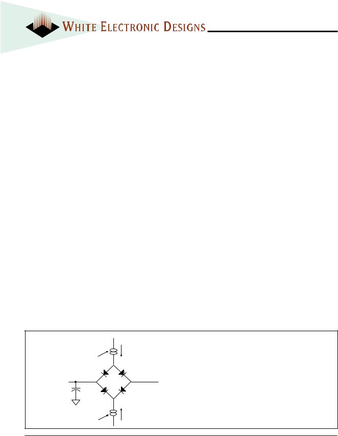
FIG. 3
AC TEST CIRCUIT
I OL
Current Source
D.U.T. |
VZ ≈1.5V |
Ceff = 50 pf |
(Bipolar Supply) |
|
IOH
Current Source
AC TEST CONDITIONS
Parameter |
Typ |
Unit |
Input Pulse Levels |
VIL = 0, VIH = 3.0 |
V |
|
|
|
Input Rise and Fall |
5 |
ns |
Input and Output Reference Level |
1.5 |
V |
|
|
|
Output Timing Reference Level |
1.5 |
V |
|
|
|
NOTES:
VZ is programmable from -2V to +7V. IOL & IOH programmable from 0 to 16mA. Tester Impedance Z0 = 75 Ω.
VZ is typically the midpoint of VOH and VOL.
IOL & IOH are adjusted to simulate a typical resistive load circuit. ATE tester includes jig capacitance.
White Electronic Designs Corporation • Phoenix, AZ • (602) 437-1520 |
4 |

|
|
|
|
|
WSE128K16-XXX |
FIG. 4 |
SRAM READ CYCLE |
|
|
|
tRC |
|
|
|
|
|
|
|
|
|
ADDRESS |
|
|
|
|
|
|
tAA |
|
|
|
|
SCS |
|
|
|
tRC |
|
|
tACS |
tCHZ |
|
|
|
|
||
ADDRESS |
|
|
|
|
|
|
|
|
tCLZ |
|
|
|
tAA |
|
|
|
|
|
|
SOE |
|
|
|
|
|
|
|
|
|
|
tOH |
|
|
tOE |
tOHZ |
SRAM |
|
|
SRAM |
tOLZ |
|
DATA I/O |
PREVIOUS DATA VALID |
DATA VALID |
DATA I/O |
HIGH IMPEDANCE |
DATA VALID |
|
|
|
|
|
|
|
READ CYCLE 1, (SCS = OE = VIL, SWE = VIH) |
|
READ CYCLE 2, (SWE = VIH) |
||
FIG. 5 SRAM WRITE CYCLE
SWE CONTROLLED
|
tWC |
|
ADDRESS |
|
|
tAW |
|
tAH |
|
tCW |
|
|
|
|
SCS |
|
|
tAS |
tWP |
|
|
|
|
SWE |
|
tOW |
|
|
|
tWHZ |
tDW |
tDH |
SRAM |
|
|
DATA I/O |
DATA VALID |
|
WRITE CYCLE 1, SWE CONTROLLED
FIG. 6 SRAM WRITE CYCLE
SCS CONTROLLED
tWC
ADDRESS
tAS |
tAW |
tAH |
|
tCW |
|||
|
|
||
SCS |
|
|
|
|
tWP |
|
|
SWE |
|
|
|
|
tDW |
tDH |
SRAM
DATA I/O |
|
DATA VALID |
|
WRITE CYCLE 2, SCS CONTROLLED
5 |
White Electronic Designs Corporation • (602) 437-1520 • www.whiteedc.com |
 Loading...