


White Electronic Designs WF4M16-150DTC5A, WF4M16-150DTC5, WF4M16-120DTM5A, WF4M16-120DTM5, WF4M16-120DTI5A Datasheet
...
WF4M16-XDTX5
HI-RELIABILITY PRODUCT
2x2Mx16 5V FLASH MODULE ADVANCED*
FEATURES
■Access Time of 90, 120, 150ns
■Packaging:
•56 Lead, Hermetic Ceramic, 0.520" CSOP (Package 213). Fits standard 56 SSOP footprint.
■Sector Architecture
•32 equal size sectors of 64KBytes per each 2Mx8 chip
•Any combination of sectors can be erased. Also supports full chip erase.
■Minimum 100,000 Write/Erase Cycles Minimum
■Organized as two banks of 2Mx16; User Configurable as 4 x 2Mx8
■Commercial, Industrial, and Military Temperature Ranges
■5 Volt Read and Write. 5V ± 10% Supply.
■Low Power CMOS
■Data Polling and Toggle Bit feature for detection of program or erase cycle completion.
■Supports reading or programming data to a sector not being erased.
■Built-in Decoupling Caps and Multiple Ground Pins for Low Noise Operation, Separate Power and Ground Planes to improve noise immunity
■RESET pin resets internal state machine to the read mode.
■Ready/Busy (RY/BY) output for direction of program or erase cycle completion.
*This data sheet describes a product that may or may not be under development and is subject to change or cancellation without notice.
Note: For programming information refer to Flash Programming 16M5 Application Note.
FIG. 1 PIN CONFIGURATION FOR WF4M16-XDTX5 |
|
|
|
|
|
|
|
|
|
|
|
|
|
|
|
|
|||||||||||||||||||||||||||||||||||||
|
|
|
|
|
|
56 CSOP |
|
|
|
|
|
|
|
|
|
|
|
|
|
|
|
|
|
|
|
|
|
|
|
|
|
|
|
|
|
|
|
|
|
|
|
|
|
PIN DESCRIPTION |
|||||||||
|
|
|
|
|
|
TOP VIEW |
|
|
|
|
|
|
|
|
|
|
|
|
|
|
|
|
|
|
|
|
|
|
|
|
|
|
|
|
|
|
|
|
|
|
|
|
|
|
|
|
|
|
|
|
|
||
|
|
|
|
|
|
|
|
|
|
|
|
|
|
|
|
|
|
|
|
|
|
|
|
|
|
|
|
|
|
|
|
|
|
|
|
|
|
|
|
|
|
|
I/O0-15 |
|
Data Inputs/Outputs |
|
|||||||
|
|
|
|
|
|
|
|
|
|
|
|
|
|
|
|
|
|
|
|
|
|
|
|
|
|
|
|
|
|
|
|
|
|
|
|
|
|
|
|
|
|
|
|
|
|
|
|
||||||
CS1 |
|
1 |
56 |
|
NC |
|
|
|
|
|
|
|
|
|
|
|
|
|
|
|
BLOCK DIAGRAM |
|
|
|
|
|
|
|
|
|
|
|
|
||||||||||||||||||||
|
|
|
|
|
|
|
|
|
|
|
|
|
|
|
|
|
|
|
|
|
|
|
|
|
|
|
|
||||||||||||||||||||||||||
|
A12 |
|
|
|
2 |
55 |
|
RESET |
|
|
|
|
|
|
|
|
|
|
|
|
|
|
|
|
|
|
|
|
A0-20 |
|
Address Inputs |
|
|||||||||||||||||||||
|
|
|
|
|
|
|
|
|
|
|
|
|
|
|
|
|
|
|
|
|
|
|
|
|
|
||||||||||||||||||||||||||||
|
A13 |
3 |
54 |
|
A11 |
|
|
|
|
|
|
|
|
|
|
|
|
|
|
|
|
|
|
|
|
|
|
|
|
|
|
|
|
|
|
|
|
|
|
|
|
|
|
|
|
||||||||
|
|
|
|
|
|
|
|
|
|
|
|
|
|
|
|
|
|
|
|
|
|
|
|
|
|
|
|
|
|
|
|
|
|
|
|
|
|
|
|
||||||||||||||
|
A14 |
4 |
53 |
|
A10 |
|
|
|
|
|
|
|
|
|
|
|
|
|
|
|
I / O 0 - 7 |
|
|
I/O 8 - 1 5 |
|
|
|
|
|
|
|
|
WE |
|
Write Enable |
|
|||||||||||||||||
|
A15 |
5 |
52 |
|
|
|
|
|
|
|
|
|
|
|
|
|
|
|
|
|
|
|
|
|
|
|
|
|
|
|
|
||||||||||||||||||||||
|
|
A9 |
|
|
|
|
|
|
|
|
|
|
|
|
|
|
|
|
|
|
|
|
|
|
|
|
|
|
|
|
|
|
|
|
|
|
|
|
|
|
|
|
|||||||||||
|
|
|
|
|
|
|
|
|
|
|
|
|
|
|
|
|
|
|
|
|
|
|
|
|
|
|
|
|
|
|
|
|
|
|
|
|
|
Chip Selects |
|
||||||||||||||
|
NC |
6 |
51 |
|
A1 |
|
|
RESET |
|
|
|
|
|
|
|
|
|
|
|
|
|
|
|
|
|
|
|
|
|
|
|
|
|
|
|
CS |
1-4 |
|
|
|
|||||||||||||
|
|
|
|
|
|
7 |
50 |
|
|
|
|
|
|
|
|
|
|
|
|
|
|
|
|
|
|
|
|
|
|
|
|
|
|
|
|
|
|
|
|
|
|
|
|
|
|
||||||||
CS2 |
|
A2 |
|
|
|
|
WE |
|
|
|
|
|
|
|
|
|
|
|
|
|
|
|
|
|
|
|
|
|
|
|
|||||||||||||||||||||||
|
|
|
|
|
|
|
|
|
|
|
|
|
|
|
|
|
|
|
|
Output Enable |
|
||||||||||||||||||||||||||||||||
|
NC |
8 |
49 |
|
A3 |
|
|
|
|
|
|
|
|
|
|
|
|
|
|
|
|
|
|
|
|
|
|
|
|
|
|
|
|
|
|
|
|
OE |
|
|
|
|
|||||||||||
|
|
|
|
OE |
|
|
|
|
|
|
|
|
|
|
|
|
|
|
|
|
|
|
|||||||||||||||||||||||||||||||
|
|
|
|
|
|
|
|
|
|
|
|
|
|
|
|
|
|
|
|
|
|
|
|
|
|
|
|
|
|
|
|
|
|
||||||||||||||||||||
|
A20 |
9 |
48 |
|
A4 |
|
|
A 0 - 2 0 |
|
|
|
|
|
|
|
|
|
|
|
|
|
|
|
|
|
|
|
|
|
VCC |
|
Power Supply |
|
||||||||||||||||||||
|
A19 |
10 |
47 |
|
A5 |
|
|
|
|
|
|
|
|
|
|
|
|
|
|
|
|
|
|
|
|
|
|
|
|
|
|
|
|
|
|
|
|
|
|
||||||||||||||
|
|
RY/BY |
|
|
|
|
|
|
|
|
|
|
|
|
|
|
|
|
|||||||||||||||||||||||||||||||||||
|
A18 |
11 |
46 |
|
A6 |
|
|
|
|
|
|
|
|
|
|
|
|
|
|
|
|
|
|
|
|
|
|
|
|
|
|
|
|
|
|
|
|
GND |
|
Ground |
|
||||||||||||
|
A17 |
12 |
45 |
|
A7 |
|
|
|
|
|
|
|
|
|
|
|
|
2M x 8 |
|
|
2M x 8 |
|
2M x 8 |
|
2M x 8 |
|
|
||||||||||||||||||||||||||
|
A16 |
13 |
44 |
|
GND |
|
|
|
|
|
|
|
|
|
|
|
|
|
|
|
|
|
|
|
|
|
|
|
|
||||||||||||||||||||||||
|
|
|
|
|
|
Ready/Busy |
|
||||||||||||||||||||||||||||||||||||||||||||||
|
VCC |
14 |
43 |
|
A8 |
|
|
|
|
|
|
|
|
|
|
|
|
|
|
|
|
|
|
|
|
|
|
|
|
|
|
|
|
|
|
|
|
RY/BY |
|
|
|
||||||||||||
GND |
15 |
42 |
|
VCC |
|
|
|
|
|
|
|
|
|
|
|
|
|
|
|
|
|
|
|
|
|
|
|
|
|
|
|
|
|
|
|
|
|
|
|
|
|
|
|
|
|||||||||
I/O6 |
16 |
41 |
|
I/O9 |
|
|
|
|
|
|
|
|
|
|
|
|
|
|
|
|
|
|
|
|
|
|
|
|
|
|
|
|
|
|
|
|
RESET |
|
Reset |
|
|||||||||||||
|
|
|
CS1 |
|
|
|
|
|
|
|
|
|
|
|
|
|
|
|
|
|
|
|
|
|
|
|
|
|
|
||||||||||||||||||||||||
I/O14 |
17 |
40 |
|
I/O1 |
|
|
|
|
|
|
|
|
|
|
|
|
|
|
|
|
|
|
|
|
|
|
|
|
|
|
|
|
|
|
|
|
|
||||||||||||||||
|
|
|
|
|
|
|
|
|
|
|
|
|
|
|
|
|
|
|
|
|
|
|
|
|
|
|
|
|
|
|
|
|
|
|
|
|
|
|
|
|
|||||||||||||
|
|
|
CS2 |
|
|
|
|
|
|
|
|
|
|
|
|
|
|
|
|
|
|
|
|
|
|
|
|
|
|
|
|
|
|
|
|
|
|||||||||||||||||
I/O7 |
|
|
18 |
39 |
|
I/O8 |
|
|
|
|
|
|
|
|
|
|
|
|
|
|
|
|
|
|
|
|
|
|
|
|
|
|
|
|
|
|
|
||||||||||||||||
|
|
|
|
|
|
|
|
|
|
|
|
|
|
|
|
|
|
|
|
|
|
|
|
|
|
|
|
|
|
|
|
|
|
|
|
|
|
|
|
|
|
|
|||||||||||
|
|
|
CS3 |
|
|
|
|
|
|
|
|
|
|
|
|
|
|
|
|
|
|
|
|
|
|
|
|
|
|
|
|
|
|
|
|
|
|
||||||||||||||||
I/O15 |
19 |
38 |
|
I/O0 |
|
|
|
|
|
|
|
|
|
|
|
|
|
|
|
|
|
|
|
|
|
|
|
|
|
|
|
|
|
|
|
|
|
|
|
|
|
||||||||||||
|
|
|
|
|
|
|
|
|
|
|
|
|
|
|
|
|
|
|
|
|
|
|
|
|
|
|
|
|
|
|
|
|
|
|
|
|
|
|
|
|
|||||||||||||
|
|
|
CS4 |
|
|
|
|
|
|
|
|
|
|
|
|
|
|
|
|
|
|
|
|
|
|
||||||||||||||||||||||||||||
|
|
|
20 |
37 |
|
A0 |
|
|
|
|
|
|
|
|
|
|
|
|
|
|
|
|
|
|
|
|
|
|
|
|
|
|
|
|
|
|
|
|
|
|
|
|
|
|
|
|
|||||||
RY/BY |
|
|
|
|
|
|
|
|
|
|
|
|
|
|
|
|
|
|
|
|
|
|
|
|
|
|
|
|
|
|
|
|
|
|
|
|
|
|
|
|
|
||||||||||||
|
OE |
|
21 |
36 |
|
NC |
NOTE: |
|
|
|
|
|
|
|
|
|
|
|
|
|
|
|
|
|
|
|
|
|
|
||||||||||||||||||||||||
|
|
|
22 |
35 |
|
|
|
|
|
|
|
|
|
|
|
|
|
|
|
|
|
|
|
|
|
|
|
|
|
|
|
|
|
|
|
|
|
|
|
|
|
|
|
|
|
|
|
|
|||||
|
WE |
|
|
CS3 |
|
|
|
|
|
|
|
|
|
|
|
|
|
|
|
|
|
|
|
|
|
|
|
|
|
|
|
|
|
|
|
|
|
|
|
|
|
|
|
|
|||||||||
1. RY/BY is an open drain output and should be pulled-up to Vcc with an |
|
|
|
||||||||||||||||||||||||||||||||||||||||||||||||||
|
NC |
23 |
34 |
|
|
|
|
|
|
|
|
||||||||||||||||||||||||||||||||||||||||||
|
|
CS4 |
|
|
|
||||||||||||||||||||||||||||||||||||||||||||||||
I/O13 |
24 |
33 |
|
I/O2 |
external resistor. |
|
|
|
|
|
|
|
|
|
|
|
|
|
|
|
|
|
|
|
|
|
|
||||||||||||||||||||||||||
I/O5 |
25 |
32 |
|
I/O10 |
|
|
|
|
|
|
|
|
|
|
|
|
|
|
|
|
|
|
|
|
|
|
|
|
|
|
|
|
|
|
|
|
|
|
|
|
|
|
|
|
|||||||||
2. CS1 and CS3 control the same data bus. Reads cannot be done with CS1 |
|
|
|
||||||||||||||||||||||||||||||||||||||||||||||||||
I/O12 |
26 |
31 |
|
I/O3 |
|
|
|
||||||||||||||||||||||||||||||||||||||||||||||
|
|
|
|
|
|
|
|
|
|
|
|
|
|
|
|
|
|
|
|
|
|
|
|
|
|
|
|
|
|
|
|
|
|
|
|
|
|
|
|
|
|||||||||||||
I/O4 |
27 |
30 |
|
I/O11 |
and CS3 both active. CS2 and CS4 control the same data bus. Reads |
|
|
|
|||||||||||||||||||||||||||||||||||||||||||||
|
VCC |
28 |
29 |
|
GND |
cannot be done with |
CS |
2 and |
CS |
4 both active. |
|
|
|
|
|
|
|
|
|
|
|
|
|||||||||||||||||||||||||||||||
|
|
|
|
|
|
|
|
|
|
|
|
|
|
3. Address compatible with Intel 2M8 56 SSOP. |
|
|
|
|
|
|
|
|
|
|
|
|
|||||||||||||||||||||||||||
|
|
|
|
|
|
|
|
|
|
|
|
|
|
|
|
|
|
|
|
|
|
|
|
|
|
|
|
|
|
|
|
|
|
|
|
|
|
|
|
|
|
|
|
|
|
|
|
|
|
|
|
|
|
November 1999 Rev.3 |
1 |
White Electronic Designs Corporation • (602) 437-1520 • www.whiteedc.com |

WF4M16-XDTX5
ABSOLUTE MAXIMUM RATINGS
Parameter |
Symbol |
Ratings |
Unit |
Voltage on Any Pin Relative to VSS |
VT |
-2.0 to +7.0 |
V |
Power Dissipation |
PT |
8 |
W |
Storage Temperature |
Tstg |
-65 to +125 |
°C |
Short Circuit Output Current |
IOS |
100 |
mA |
Endurance - Write/Erase Cycles |
|
100,000 min |
cycles |
(Mil Temp) |
|
|
|
Data Retention (Mil Temp) |
|
20 |
years |
CAPACITANCE
(TA = +25°C)
|
Parameter |
Symbol |
Conditions |
Max |
Unit |
||||
|
|
|
|
|
|
|
|
|
|
|
|
|
|
|
capacitance |
COE |
VIN = 0 V, f = 1.0 MHz |
45 |
pF |
|
OE |
|
|||||||
|
|
|
|
|
capacitance |
CWE |
VIN = 0 V, f = 1.0 MHz |
45 |
pF |
|
WE |
||||||||
|
|
|
capacitance |
CCS |
VIN = 0 V, f = 1.0 MHz |
15 |
pF |
||
|
CS |
||||||||
|
Data I/O capacitance |
CI/O |
VI/O = 0 V, f = 1.0 MHz |
25 |
pF |
||||
|
Address input capacitance |
CAD |
VIN = 0 V, f = 1.0 MHz |
45 |
pF |
||||
This parameter is guaranteed by design but not tested.
RECOMMENDED DC OPERATING CONDITIONS
Parameter |
Symbol |
Min |
Max |
Unit |
|
|
|
|
|
Supply Voltage |
VCC |
4.5 |
5.5 |
V |
Ground |
VSS |
0 |
0 |
V |
Input High Voltage |
VIH |
2.0 |
VCC + 0.5 |
V |
Input Low Voltage |
VIL |
-0.5 |
+0.8 |
V |
Operating Temperature (Mil.) |
TA |
-55 |
+125 |
°C |
Operating Temperature (Ind.) |
TA |
-40 |
+85 |
°C |
DC CHARACTERISTICS - CMOS COMPATIBLE
(VCC = 5.0V, VSS = 0V, TA = -55°C to +125°C)
Parameter |
Symbol |
|
|
|
|
|
|
|
|
|
Conditions |
Min |
Max |
Unit |
Input Leakage Current |
ILI |
|
VCC = 5.5, VIN = GND to VCC |
|
10 |
A |
||||||||
Output Leakage Current |
ILOx32 |
|
VCC = 5.5, VIN = GND to VCC |
|
10 |
A |
||||||||
VCC Active Current for Read (1) |
ICC1 |
|
|
= VIL, |
|
|
|
|
= VIH, f = 5MHz, VCC = 5.5 |
|
82 |
mA |
||
|
CS |
OE |
|
|||||||||||
VCC Active Current for Program or Erase (2) |
ICC2 |
|
|
|
|
|
|
|
= VIH, VCC = 5.5 |
|
122 |
mA |
||
|
CS |
= VIL, |
OE |
|
||||||||||
VCC Standby Current |
ICC3 |
|
VCC = 5.5, |
|
= VIH, f = 5MHz |
|
8.0 |
mA |
||||||
|
CS |
|
||||||||||||
Output Low Voltage |
VOL |
|
IOL = 12.0 mA, VCC = 4.5 |
|
0.45 |
V |
||||||||
Output High Voltage |
VOH |
|
IOH = -2.5 mA, VCC = 4.5 |
0.85xVcc |
|
V |
||||||||
Low VCC Lock-Out Voltage |
VLKO |
|
|
|
|
|
|
|
|
|
|
3.2 |
4.2 |
V |
|
|
|
|
|
|
|
|
|
|
|
|
|
|
|
NOTES:
1.The Icc current listed includes both the DC operating current and the frequency dependent component (@ 5MHz). The frequency component typically is less than 2mA/MHz, with OE at VIH.
2.Icc active while Embedded Algorithm (program or erase) is in progress.
3.DC test conditions VIL = 0.3V, VIH = VCC - 0.3V
White Electronic Designs Corporation • (602) 437-1520 • www.whiteedc.com |
2 |

WF4M16-XDTX5
AC CHARACTERISTICS – WRITE/ERASE/PROGRAM OPERATIONS - WE CONTROLLED
(VCC = 5.0V, TA = -55°C to +125°C)
Parameter |
Symbol |
-90 |
|
|
-120 |
|
-150 |
Unit |
||||
|
|
|
Min |
Max |
Min |
|
Max |
Min |
|
Max |
|
|
Write Cycle Time |
tAVAV |
tWC |
90 |
|
|
120 |
|
|
150 |
|
|
ns |
|
|
|
|
|
|
|
|
|
|
|
|
|
Chip Select Setup Time |
tELWL |
tCS |
0 |
|
|
0 |
|
|
0 |
|
|
ns |
|
|
|
|
|
|
|
|
|
|
|
|
|
Write Enable Pulse Width |
tWLWH |
tWP |
45 |
|
|
50 |
|
|
50 |
|
|
ns |
|
|
|
|
|
|
|
|
|
|
|
|
|
Address Setup Time |
tAVWL |
tAS |
0 |
|
|
0 |
|
|
0 |
|
|
ns |
|
|
|
|
|
|
|
|
|
|
|
|
|
Data Setup Time |
tDVWH |
tDS |
45 |
|
|
50 |
|
|
50 |
|
|
ns |
|
|
|
|
|
|
|
|
|
|
|
|
|
Data Hold Time |
tWHDX |
tDH |
0 |
|
|
0 |
|
|
0 |
|
|
ns |
|
|
|
|
|
|
|
|
|
|
|
|
|
Address Hold Time |
tWLAX |
tAH |
45 |
|
|
50 |
|
|
50 |
|
|
ns |
|
|
|
|
|
|
|
|
|
|
|
|
|
Write Enable Pulse Width High |
tWHWL |
tWPH |
20 |
|
|
20 |
|
|
20 |
|
|
ns |
|
|
|
|
|
|
|
|
|
|
|
|
|
Duration of Byte Programming Operation (1) |
tWHWH1 |
|
|
|
300 |
|
|
300 |
|
|
300 |
s |
|
|
|
|
|
|
|
|
|
|
|
|
|
Sector Erase (2) |
tWHWH2 |
|
|
|
15 |
|
|
15 |
|
|
15 |
sec |
|
|
|
|
|
|
|
|
|
|
|
|
|
Read Recovery Time before Write |
tGHWL |
|
0 |
|
|
0 |
|
|
0 |
|
|
s |
|
|
|
|
|
|
|
|
|
|
|
|
|
VCC Setup Time |
tVCS |
|
50 |
|
|
50 |
|
|
50 |
|
|
s |
|
|
|
|
|
|
|
|
|
|
|
|
|
Chip Programming Time |
|
|
|
|
44 |
|
|
44 |
|
|
44 |
sec |
|
|
|
|
|
|
|
|
|
|
|
|
|
Chip Erase Time (3) |
|
|
|
|
256 |
|
|
256 |
|
|
256 |
sec |
|
|
|
|
|
|
|
|
|
|
|
|
|
Output Enable Hold Time (4) |
|
tOEH |
10 |
|
|
10 |
|
|
10 |
|
|
ns |
|
|
|
|
|
|
|
|
|
|
|
|
|
NOTES:
1.Typical value for tWHWH1 is 7 s.
2.Typical value for tWHWH2 is 1sec.
3.Typical value for Chip Erase Time is 32sec.
4.For Toggle and Data Polling.
AC CHARACTERISTICS – READ-ONLY OPERATIONS
(VCC = 5.0V, TA = -55°C to +125°C)
Parameter |
Symbol |
|
|
-90 |
|
-120 |
|
-150 |
Unit |
||||||||
|
|
|
|
|
|
|
|
Min |
|
Max |
Min |
|
Max |
Min |
|
Max |
|
Read Cycle Time |
tAVAV |
|
tRC |
90 |
|
|
120 |
|
|
150 |
|
|
ns |
||||
|
|
|
|
|
|
|
|
|
|
|
|
|
|
|
|
|
|
Address Access Time |
tAVQV |
|
tACC |
|
|
90 |
|
|
120 |
|
|
150 |
ns |
||||
|
|
|
|
|
|
|
|
|
|
|
|
|
|
|
|
|
|
Chip Select Access Time |
tELQV |
|
tCE |
|
|
90 |
|
|
120 |
|
|
150 |
ns |
||||
|
|
|
|
|
|
|
|
|
|
|
|
|
|
|
|
|
|
Output Enable to Output Valid |
tGLQV |
|
tOE |
|
|
40 |
|
|
50 |
|
|
55 |
ns |
||||
|
|
|
|
|
|
|
|
|
|
|
|
|
|
|
|
|
|
Chip Select High to Output High Z (1) |
tEHQZ |
|
tDF |
|
|
20 |
|
|
30 |
|
|
35 |
ns |
||||
|
|
|
|
|
|
|
|
|
|
|
|
|
|
|
|
|
|
Output Enable High to Output High Z (1) |
tGHQZ |
|
tDF |
|
|
20 |
|
|
30 |
|
|
35 |
ns |
||||
|
|
|
|
|
|
|
|
|
|
|
|
|
|
|
|
|
|
Output Hold from Addresses, |
|
or |
|
Change, |
tAXQX |
|
tOH |
0 |
|
|
0 |
|
|
0 |
|
|
ns |
CS |
OE |
|
|
|
|
|
|
|
|||||||||
whichever is First |
|
|
|
|
|
|
|
|
|
|
|
|
|
||||
|
|
|
|
|
|
|
|
|
|
|
|
|
|
|
|
|
|
1. Guaranteed by design, not tested.
3 |
White Electronic Designs Corporation • (602) 437-1520 • www.whiteedc.com |
WF4M16-XDTX5
AC CHARACTERISTICS – WRITE/ERASE/PROGRAM OPERATIONS,CS CONTROLLED
(VCC = 5.0V, VSS = 0V, TA = -55°C to +125°C)
Parameter |
Symbol |
|
-90 |
|
|
-120 |
|
-150 |
Unit |
||||
|
|
|
|
Min |
Max |
Min |
|
Max |
Min |
|
Max |
|
|
Write Cycle Time |
tAVAV |
|
tWC |
90 |
|
|
120 |
|
|
150 |
|
|
ns |
Write Enable Setup Time |
tWLEL |
|
tWS |
0 |
|
|
0 |
|
|
0 |
|
|
ns |
Chip Select Pulse Width |
tELEH |
|
tCP |
45 |
|
|
50 |
|
|
50 |
|
|
ns |
Address Setup Time |
tAVEL |
|
tAS |
0 |
|
|
0 |
|
|
0 |
|
|
ns |
Data Setup Time |
tDVEH |
|
tDS |
45 |
|
|
50 |
|
|
50 |
|
|
ns |
Data Hold Time |
tEHDX |
|
tDH |
0 |
|
|
0 |
|
|
0 |
|
|
ns |
Address Hold Time |
tELAX |
|
tAH |
45 |
|
|
50 |
|
|
50 |
|
|
ns |
Chip Select Pulse Width High |
tEHEL |
|
tCPH |
20 |
|
|
20 |
|
|
20 |
|
|
ns |
Duration of Byte Programming Operation (1) |
tWHWH1 |
|
|
|
|
300 |
|
|
300 |
|
|
300 |
µs |
Sector Erase Time (2) |
tWHWH2 |
|
|
|
|
15 |
|
|
15 |
|
|
15 |
sec |
Read Recovery Time |
tGHEL |
|
|
0 |
|
|
0 |
|
|
0 |
|
|
µs |
Chip Programming Time |
|
|
|
|
|
44 |
|
|
44 |
|
|
44 |
sec |
Chip Erase Time (3) |
|
|
|
|
|
256 |
|
|
256 |
|
|
256 |
sec |
Output Enable Hold Time (4) |
|
|
tOEH |
10 |
|
|
10 |
|
|
10 |
|
|
ns |
|
|
|
|
|
|
|
|
|
|
|
|
|
|
NOTES:
1.Typical value for tWHWH1 is 7µs.
2.Typical value for tWHWH2 is 1sec.
3.Typical value for Chip Erase Time is 32sec.
4.For Toggle and Data Polling.
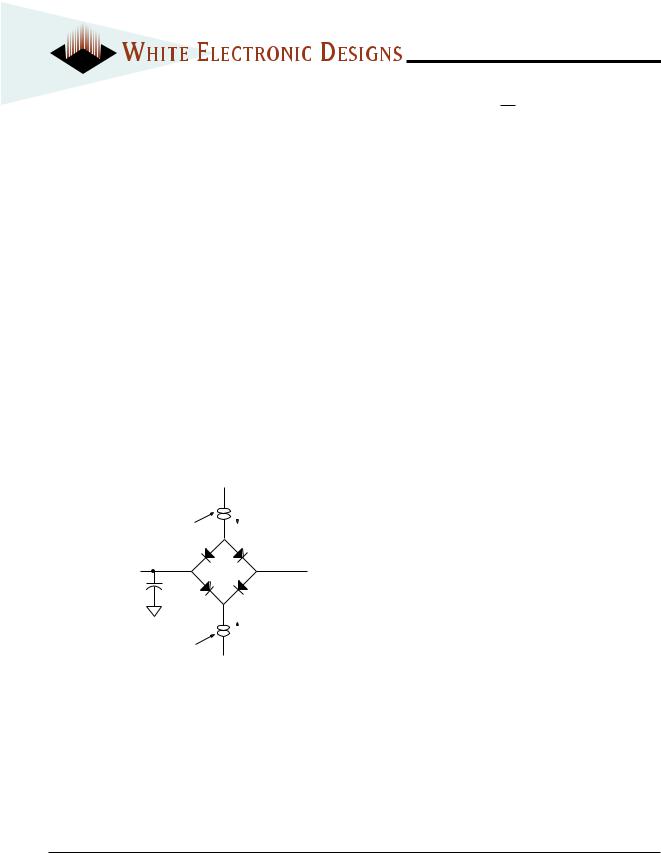
FIG. 2 |
|
|
AC TEST CONDITIONS |
|
|
|
AC TEST CIRCUIT |
|
|
|
|
|
|
I OL |
|
Parameter |
Typ |
Unit |
|
|
|
|
|
||||
Current Source |
|
|
Input Pulse Levels |
VIL = 0, VIH = 3.0 |
V |
|
|
|
|
Input Rise and Fall |
5 |
ns |
|
|
|
|
Input and Output Reference Level |
1.5 |
V |
|
D.U.T. |
|
VZ ≈1.5V |
Output Timing Reference Level |
1.5 |
V |
|
Ceff = 50 pf |
|
(Bipolar Supply) |
NOTES: |
|
|
|
|
|
|
|
|
||
|
|
|
VZ is programmable from -2V to +7V. |
|
|
|
|
|
|
IOL & IOH programmable from 0 to 16mA. |
|
|
|
|
|
|
Tester Impedance Z0 = 75 Ω. |
|
|
|
|
IOH |
|
VZ is typically the midpoint of VOH and VOL. |
|
|
|
Current Source |
|
|
IOL & IOH are adjusted to simulate a typical resistive load circuit. |
|||
|
|
|||||
|
|
ATE tester includes jig capacitance. |
|
|
|
|
|
|
|
|
|
|
|
|
|
|
|
|
|
|
White Electronic Designs Corporation • (602) 437-1520 • www.whiteedc.com |
4 |
 Loading...