


WMF2M8-150DLM5
White Electronic Designs WMF2M8-150DLM5, WMF2M8-150DLI5A, WMF2M8-150DLI5, WMF2M8-150DLC5A, WMF2M8-150DLC5 Datasheet
...
1
White Electronic Designs Corporation • (602) 437-1520 • www.whiteedc.com
HI-RELIABILITY PRODUCT
WMF2M8-XXX5
FIG. 1 PIN CONFIGURATION FOR WMF2M8-XXX5
December 1999 Rev. 4
2Mx8 MONOLITHIC FLASH, SMD 5962-97609
PRELIMINARY*
■ 5 Volt Read and Write. 5V ± 10% Supply.
■ Low Power CMOS
■ Data Polling and Toggle Bit feature for detection of program
or erase cycle completion.
■ Supports reading or programming data to a sector not being
erased.
■ RESET pin resets internal state machine to the read mode.
■ Multiple Ground Pins for Low Noise Operation
* This data sheet describes a product under development, not fully
characterized, and is subject to change without notice.
** Package to be developed.
Note: For programming information refer to Flash Programming 16M5
Application Note.
FEATURES
■ Access Times of 90, 120, 150ns
■ Packaging:
• 56 lead, Hermetic Ceramic, 0.520" CSOP (Package 207).
Fits standard 56 SSOP footprint.
• 44 pin Ceramic LCC**
• 44 pin Ceramic SOJ (Package 102)**
• 44 lead Ceramic Flatpack (Package 225)**
■ Sector Architecture
• 32 equal size sectors of 64KBytes each
• Any combination of sectors can be erased. Also supports
full chip erase.
■ 100,000 Write/Erase Cycles Minimum
■ Organized as 2Mx8
■ Commercial, Industrial, and Military Temperature Ranges
TOP VIEW
56 CSOP
PIN DESCRIPTION
I/O0-7 Data Inputs/Outputs
A0-20 Address Inputs
WE Write Enable
CS Chip Select
OE Output Enable
VCC Power Supply
GND Ground
RY/BY Ready/Busy
RESET Reset
1
2
3
4
5
6
7
8
9
10
11
12
13
14
15
16
17
18
19
20
21
22
23
24
25
26
27
28
56
55
54
53
52
51
50
49
48
47
46
45
44
43
42
41
40
39
38
37
36
35
34
33
32
31
30
29
CS
A12
A13
A14
A15
NC
NC
NC
A20
A19
A18
A17
A16
V
CC
GND
I/O6
NC
I/O7
NC
RY/BY
OE
WE
NC
NC
I/O5
NC
I/O4
V
CC
NC
RESET
A11
A10
A9
A1
A2
A3
A4
A5
A6
A7
GND
A8
V
CC
NC
I/O1
NC
I/O0
A0
NC
NC
NC
I/O2
NC
I/O3
NC
GND
TOP VIEW
1
2
3
4
5
6
7
8
9
10
11
12
13
14
15
16
17
18
19
20
21
22
A16
A15
A14
A13
A12
A11
A10
A9
A8
RESET
CS
GND
NC
WE
A7
A6
A5
A4
A3
A2
A1
A0
A17
A18
OE
I/O0
I/O1
I/O2
I/O3
I/O4
I/O5
I/O6
I/O7
V
CC
NC
NC
NC
NC
NC
NC
NC
NC
A19
A20
44
43
42
41
40
39
38
37
36
35
34
33
32
31
30
29
28
27
26
25
24
23
44 CSOJ**
44 FLATPACK**
** Package to be developed.
TOP VIEW
44 CLCC**
7
8
9
10
11
12
13
14
15
16
17
39
38
37
36
35
34
33
32
31
30
29
4365 21
44 43 42 41 40
18 19 20 21 22 23 24
25 26 27 28
A
7
A
6
A
5
A
4
NC
NC
NC
A
3
A
2
A
1
A
0
I/O0I/O1I/O2I/O
3
GND
GND
V
CC
I/O4I/O5I/O6I/O
7
A
16
A
17
A
18
A
19
NC
NC
NC
A
20
WE
OE
RY/BY
A8A9A10A11RESET
VCCCS
A12A13A14A
15
2
White Electronic Designs Corporation • (602) 437-1520 • www.whiteedc.com
WMF2M8-XXX5
ABSOLUTE MAXIMUM RATINGS
Parameter Symbol Ratings Unit
Voltage on Any Pin Relative to VSS VT -2.0 to +7.0 V
Power Dissipation PT 8W
Storage Temperature Tstg -65 to +125 °C
Short Circuit Output Current IOS 100 mA
Endurance - Write/Erase Cycles 100,000 min cycles
(Mil Temp)
Data Retention (Mil Temp) 20 years
RECOMMENDED DC OPERATING CONDITIONS
Parameter Symbol Min Typ Max Unit
Supply Voltage VCC 4.5 5.0 5.5 V
Ground VSS 00 0V
Input High Voltage VIH 2.0 - VCC + 0.5 V
Input Low Voltage VIL -0.5 - +0.8 V
Operating Temperature (Mil.) TA -55 - +125 °C
Operating Temperature (Ind.) T
A -40 - +85 °C
DC CHARACTERISTICS - CMOS COMPATIBLE
(VCC = 5.0V, VSS = 0V, TA = -55°C to +125°C)
NOTES:
1. The Icc current listed includes both the DC operating current and the frequency dependent component (@ 5MHz). The frequency component typically is
less than 2mA/MHz, with OE at VIH.
2. Icc active while Embedded Algorithm (program or erase) is in progress.
3. DC test conditions V
IL = 0.3V, VIH = VCC - 0.3V
Parameter Symbol Conditions Min Max Unit
Input Leakage Current ILI VCC = 5.5, VIN = GND to VCC 10 µA
Output Leakage Current ILO VCC = 5.5, VIN = GND to VCC 10 µA
VCC Active Current for Read (1) ICC1 CS = VIL, OE = VIH, f = 5MHz 40 mA
VCC Active Current for Program or Erase (2) ICC2 CS = VIL, OE = VIH 60 mA
VCC Standby Current ICC3 VCC = 5.5, CS = VIH, f = 5MHz, RESET = Vcc ± 0.3V 2.0 mA
Output Low Voltage VOL IOL = 12.0 mA, VCC = 4.5 0.45 V
Output High Voltage VOH IOH = -2.5 mA, VCC = 4.5 0.85xVCC V
Low VCC Lock-Out Voltage VLKO 3.2 4.2 V
CAPACITANCE
(TA = +25°C)
Parameter
Symbol
Conditions Max Unit
Address Input capacitance CAD
V
I/O
= 0 V, f = 1.0 MHz
12 pF
Output Enable capacitance COE
VIN = 0 V, f = 1.0 MHz
12 pF
Write Enable capacitance CWE
VIN = 0 V, f = 1.0 MHz
12 pF
Chip Select capacitance CCS
VIN = 0 V, f = 1.0 MHz
12 pF
Data I/O capacitance C
I/OVI/O
= 0 V, f = 1.0 MHz
12 pF
This parameter is guaranteed by design but not tested.

3
White Electronic Designs Corporation • (602) 437-1520 • www.whiteedc.com
WMF2M8-XXX5
AC CHARACTERISTICS – WRITE/ERASE/PROGRAM OPERATIONS - WE CONTROLLED
(V
CC = 5.0V, TA = -55°C to +125°C)
Parameter Symbol -90 -120 -150 Unit
Min Max Min Max Min Max
Write Cycle Time tAVAV tWC 90 120 150 ns
Chip Select Setup Time tELWL tCS 000ns
Write Enable Pulse Width tWLWH tWP 45 50 50 ns
Address Setup Time tAVWL tAS 000ns
Data Setup Time tDVWH tDS 45 50 50 ns
Data Hold Time tWHDX tDH 000ns
Address Hold Time tWLAX tAH 45 50 50 ns
Write Enable Pulse Width High tWHWL tWPH 20 20 20 ns
Duration of Byte Programming Operation (1) tWHWH1 300 300 300 µs
Sector Erase (2) tWHWH2 15 15 15 sec
Read Recovery Time before Write tGH
W
L 000µs
VCC Setup Time tVCS 50 50 50 µs
Chip Programming Time 44 44 44 sec
Chip Erase Time (3) 256 256 256 sec
Output Enable Hold Time (4) tOEH 10 10 10 ns
RESET Pulse Width t
RP 500 500 500 ns
NOTES:
1. Typical value for t
WHWH1 is 7µs.
2. Typical value for t
WHWH2 is 1sec.
3. Typical value for Chip Erase Time is 32sec.
4. For Toggle and Data Polling.
AC CHARACTERISTICS – READ-ONLY OPERATIONS
(V
CC = 5.0V, TA = -55°C to +125°C)
Parameter Symbol -90 -120 -150 Unit
Min Max Min Max Min Max
Read Cycle Time tAVAV tRC 90 120 150 ns
Address Access Time tAVQV tACC 90 120 150 ns
Chip Select Access Time tELQV tCE 90 120 150 ns
Output Enable to Output Valid tGLQV tOE 40 50 55 ns
Chip Select High to Output High Z (1) tEHQZ tDF 20 30 35 ns
Output Enable High to Output High Z (1) tGHQZ tDF 20 30 35 ns
Output Hold from Addresses, CS or OE Change, t
AXQX tOH 000ns
whichever is First
RESET Low to Read Mode (1) t
Ready 20 20 20 µs
1. Guaranteed by design, not tested.
4
White Electronic Designs Corporation • (602) 437-1520 • www.whiteedc.com
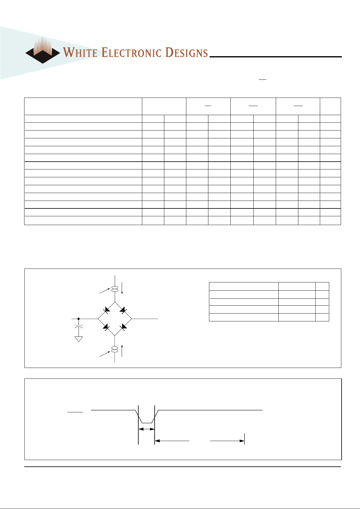
CS
WE
RY/BY
RESET
t
RP
The rising edge of the last WE signal
Entire programming
or erase operations
t
Ready
t
BUSY
AC CHARACTERISTICS – WRITE/ERASE/PROGRAM OPERATIONS,CS CONTROLLED
(V
CC = 5.0V, VSS = 0V, TA = -55°C to +125 °C)
FIG. 2
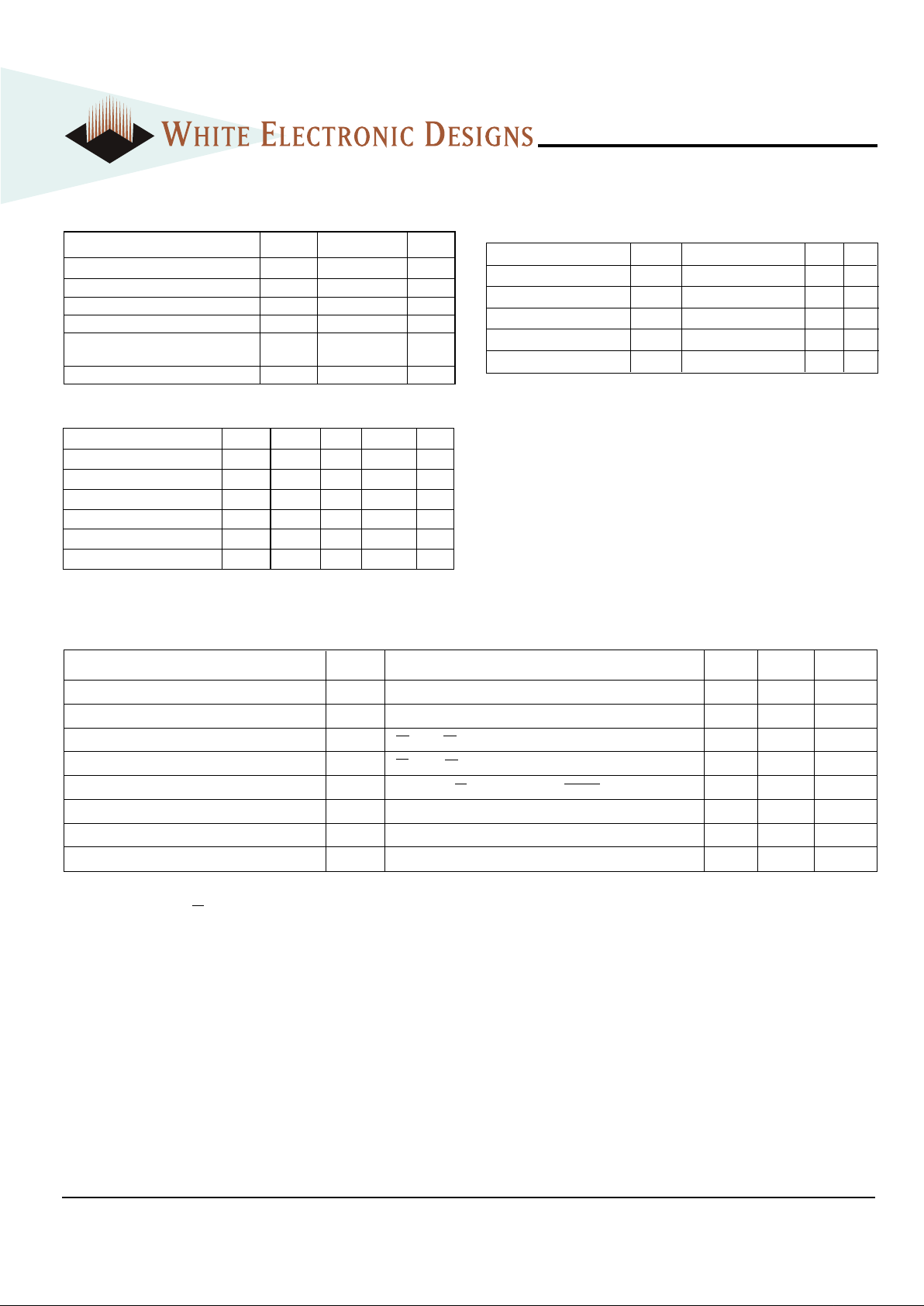
AC TEST CIRCUIT
AC TEST CONDITIONS
NOTES:
V
Z is programmable from -2V to +7V.
I
OL & IOH programmable from 0 to 16mA.
Tester Impedance Z
0 = 75 Ω.
V
Z is typically the midpoint of VOH and VOL.
I
OL & IOH
are adjusted to simulate a typical resistive load circuit.
ATE tester includes jig capacitance.
Parameter Typ Unit
Input Pulse Levels
VIL = 0, VIH = 3.0
V
Input Rise and Fall 5 ns
Input and Output Reference Level 1.5 V
Output Timing Reference Level 1.5 V
I
Current Source
D.U.T.
C = 50 pf
eff
I
OL
V ≈ 1.5V
(Bipolar Supply)
Z
Current Source
OH
Parameter Symbol -90 -120 -150 Unit
Min Max Min Max Min Max
Write Cycle Time tAVAV tWC 90 120 150 ns
Write Enable Setup Time tWLEL tWS 000ns
Chip Select Pulse Width tELEH tCP 45 50 50 ns
Address Setup Time tAVEL tAS 000ns
Data Setup Time tDVEH tDS 45 50 50 ns
Data Hold Time tEHDX tDH 000ns
Address Hold Time tELAX tAH 45 50 50 ns
Chip Select Pulse Width High tEHEL tCPH 20 20 20 ns
Duration of Byte Programming Operation (1) tWHWH1 300 300 300 µs
Sector Erase Time (2) tWHWH2 15 15 15 sec
Read Recovery Time tGHEL 000µs
Chip Programming Time 44 44 44 sec
Chip Erase Time (3) 256 256 256 sec
Output Enable Hold Time (4) t
OEH 10 10 10 ns
NOTES:
1. Typical value for tWHWH1 is 7µs.
2. Typical value for t
WHWH2 is 1sec.
3. Typical value for Chip Erase Time is 32sec.
4. For Toggle and Data Polling.
FIG. 3
RESET TIMING DIAGRAM
WMF2M8-XXX5
 Loading...