


White Electronic Designs WEDF1M32B-120HC5A, WEDF1M32B-120HC5, WEDF1M32B-120G2TM5A, WEDF1M32B-120G2TM5, WEDF1M32B-120G2TI5A Datasheet
...
1Mx32 5V FLASH MODULE ADVANCED*
FEATURES
■Access Times of 70, 90, 120ns
■Packaging:
•66 pin, PGA Type, 1.185" square, Hermetic Ceramic HIP (Package 401)
•68 lead, 22mm Low Profile CQFP, 4.6mm (0.180"), (Package 509)
■Sector Architecture
•One 16KByte Sectors
•Two 8KByte Sectors
•One 32KByte Sectors
•Fifteen 64KByte Sectors
■1,000,000 Erase/Program Cycles
WEDF1M32B-XXX5
HI-RELIABILITY PRODUCT
■Organized as 1Mx32, user configurable as 2Mx16 or 4Mx8.
■Commercial, Industrial and Military Temperature Ranges
■5V ± 10% for Read and Write Operations.
■Low Power CMOS
■Embedded Erase and Program Algorithm
■Built-in Decoupling Caps and Multiple Ground Pins for Low Noise Operation
■Weight
WEDF1M32B-XG2TX5 - 8 grams typical WEDF1M32B-XHX5 - 13 grams typical
*This data sheet describes a product that may or may not be under development and is subject to change or cancellation without notice.
FIG. 1 PIN CONFIGURATION FOR WEDF1M32B-XHX5 |
|
|
|
|||||||
|
|
TOP VIEW |
|
|
|
|
|
PIN DESCRIPTION |
||
1 |
12 |
23 |
|
34 |
45 |
|
56 |
|
|
|
I/O8 |
RESET |
I/O15 |
I/O24 |
|
VCC |
I/O31 |
|
|
I/O0-31 |
Data Inputs/Outputs |
|
|
|
A0-19 |
Address Inputs |
||||||
|
|
|
|
|
|
|
|
|
||
I/O9 |
CS2 |
I/O14 |
I/O25 |
|
CS4 |
I/O30 |
|
|
WE |
Write Enable |
|
|
|
|
|
|
|
|
|
||
I/O10 |
GND |
I/O13 |
I/O26 |
|
NC |
I/O29 |
|
|
CS1-4 |
Chip Selects |
A14 |
I/O11 |
I/O12 |
A7 |
|
I/O27 |
I/O28 |
|
|
OE |
Output Enable |
|
|
|
|
|
||||||
|
|
|
|
|
|
|
|
|
RESET |
Reset |
A16 |
A10 |
OE |
A12 |
|
A4 |
A1 |
|
|
VCC |
Power Supply |
|
|
|
|
|
|
|
|
|
||
A11 |
A9 |
A17 |
NC |
|
A5 |
A2 |
|
|
GND |
Ground |
A0 |
A15 |
WE |
A13 |
|
A6 |
A3 |
|
|
NC |
Not Connected |
|
|
|
|
|
||||||
A18 |
VCC |
I/O7 |
A8 |
|
NC |
I/O23 |
BLOCK DIAGRAM |
|
||
|
|
|
|
|
||||||
|
|
|
|
|
|
|
CS1 |
CS2 |
CS3 |
CS4 |
I/O0 |
CS1 |
I/O6 |
I/O16 |
|
CS3 |
I/O22 |
RESET |
|
|
|
|
|
|
|
|
|
|
WE |
|
|
|
I/O1 |
A19 |
I/O5 |
I/O17 |
|
GND |
I/O21 |
OE |
|
|
|
|
A 0 - 1 9 |
|
|
|
||||||
|
|
|
|
|
|
|
|
|
|
|
I/O2 |
I/O3 |
I/O4 |
I/O18 |
|
I/O19 |
I/O20 |
1M x 8 |
1M x 8 |
1M x 8 |
1M x 8 |
|
|
|
|
|
|
|
||||
11 |
22 |
33 |
|
44 |
55 |
|
66 |
|
|
|
|
|
|
|
|
|
|
8 |
8 |
8 |
8 |
|
|
|
|
|
|
|
I/O 0 - 7 |
I/O 8 - 1 5 |
I/O 1 6 - 2 3 |
I/O 2 4 - 3 1 |
May 1999 Rev. 1 |
1 |
White Electronic Designs Corporation • Phoenix, AZ • (602) 437-1520 |
WEDF1M32B-XXX5
FIG. 2 PIN CONFIGURATION FOR WEDF1M32B-XG2TX5
TOP VIEW
|
|
RESET |
A0 |
A1 |
A2 |
A3 |
A4 |
A5 |
|
|
CS3 |
|
GND |
|
CS4 |
|
WE1 |
|
A6 A7 |
|
A8 |
A9 |
A10 |
VCC |
|
||
|
|
|
|
|
|
|
|
||||||||||||||||||||
|
|
|
|
|
|
|
|||||||||||||||||||||
|
9 |
8 |
7 |
6 |
5 |
4 |
3 |
|
2 |
1 |
68 67 66 65 64 63 62 61 |
|
|||||||||||||||
I/O0 |
10 |
|
|
|
|
|
|
|
|
|
|
|
|
|
|
|
|
|
|
|
|
|
|
|
|
60 |
I/O16 |
I/O1 |
11 |
|
|
|
|
|
|
|
|
|
|
|
|
|
|
|
|
|
|
|
|
|
|
|
|
59 |
I/O17 |
I/O2 |
12 |
|
|
|
|
|
|
|
|
|
|
|
|
|
|
|
|
|
|
|
|
|
|
|
|
58 |
I/O18 |
I/O3 |
13 |
|
|
|
|
|
|
|
|
|
|
|
|
|
|
|
|
|
|
|
|
|
|
|
|
57 |
I/O19 |
I/O4 |
14 |
|
|
|
|
|
|
|
|
|
|
|
|
|
|
|
|
|
|
|
|
|
|
|
|
56 |
I/O20 |
I/O5 |
15 |
|
|
|
|
|
|
|
|
|
|
|
|
|
|
|
|
|
|
|
|
|
|
|
|
55 |
I/O21 |
I/O6 |
16 |
|
|
|
|
|
|
|
|
|
|
|
|
|
|
|
|
|
|
|
|
|
|
|
|
54 |
I/O22 |
I/O7 |
17 |
|
|
|
|
|
|
|
|
|
|
|
|
|
|
|
|
|
|
|
|
|
|
|
|
53 |
I/O23 |
GND |
18 |
|
|
|
|
|
|
|
|
|
|
|
|
|
|
|
|
|
|
|
|
|
|
|
|
52 |
GND |
I/O8 |
19 |
|
|
|
|
|
|
|
|
|
|
|
|
|
|
|
|
|
|
|
|
|
|
|
|
51 |
I/O24 |
I/O9 |
20 |
|
|
|
|
|
|
|
|
|
|
|
|
|
|
|
|
|
|
|
|
|
|
|
|
50 |
I/O25 |
I/O10 |
21 |
|
|
|
|
|
|
|
|
|
|
|
|
|
|
|
|
|
|
|
|
|
|
|
|
49 |
I/O26 |
I/O11 |
22 |
|
|
|
|
|
|
|
|
|
|
|
|
|
|
|
|
|
|
|
|
|
|
|
|
48 |
I/O27 |
I/O12 |
23 |
|
|
|
|
|
|
|
|
|
|
|
|
|
|
|
|
|
|
|
|
|
|
|
|
47 |
I/O28 |
I/O13 |
24 |
|
|
|
|
|
|
|
|
|
|
|
|
|
|
|
|
|
|
|
|
|
|
|
|
46 |
I/O29 |
I/O14 |
25 |
|
|
|
|
|
|
|
|
|
|
|
|
|
|
|
|
|
|
|
|
|
|
|
|
45 |
I/O30 |
I/O15 |
26 |
|
|
|
|
|
|
|
|
|
|
|
|
|
|
|
|
|
|
|
|
|
|
|
|
44 |
I/O31 |
|
27 28 29 30 31 32 33 34 35 36 37 38 39 40 41 42 43 |
|
|||||||||||||||||||||||||
|
|
VCC |
A11 |
A12 |
A13 |
A14 |
A15 |
A16 |
|
CS1 |
|
OE |
|
CS2 |
|
A17 |
|
WE2 |
|
WE3 |
|
WE4 |
A18 |
A19 |
NC |
|
|
|
|
|
|
|
|
|
|||||||||||||||||||||
|
|
|
|
|
|
|
|
|
|
||||||||||||||||||
|
|
|
|
|
|
|
|
|
|
|
|
|
|
|
|
|
|
|
|||||||||
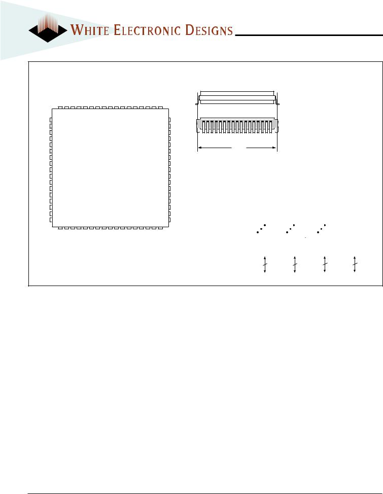
0.940"
The White 68 lead G2T CQFP fills the same fit and function as the JEDEC 68 lead CQFJ or 68 PLCC. But the G2T has the TCE and lead inspection advantage of the CQFP form.
PIN DESCRIPTION
|
I/O0-31 |
Data Inputs/Outputs |
||||||
|
|
|
|
|
|
|
|
|
|
|
A0-19 |
Address Inputs |
|||||
|
|
|
|
|
|
|
|
|
|
|
|
|
1-4 |
|
Write Enables |
||
WE |
||||||||
|
|
|
|
|
|
|
|
|
|
|
|
|
Chip Selects |
||||
|
|
CS |
1-4 |
|
||||
|
|
|
|
|
|
|
|
|
|
|
|
|
|
|
|
|
Output Enable |
|
|
|
OE |
|||||
|
|
|
|
|
|
|
|
|
|
|
|
Reset |
|||||
RESET |
||||||||
|
|
|
|
|
|
|
|
|
|
|
VCC |
Power Supply |
|||||
|
|
|
|
|
|
|
|
|
|
|
GND |
Ground |
|||||
|
|
|
NC |
Not Connected |
||||
|
|
|
|
|
|
|
|
|
BLOCK DIAGRAM
|
|
|
|
|
|
|
|
|
|
|
|
|
|
|
|
|
|
|
|
|
|
|
|
|
|
|
|
|
|
|
|
|
|
|
|
|
|
|
|
|
|
|
|
|
|
|
|
|
|
|
|
|
|
|
|
|
|
WE3 CS3 |
|
|
WE4 CS4 |
||||||||
|
|
|
|
|
|
|
|
|
WE1 CS1 |
|
|
WE2 CS2 |
|
|
|
|
||||||||||||||||||
|
|
|
|
|
|
|
|
|
|
|
|
|
|
|
|
|
|
|
|
|
|
|
|
|
|
|
|
|
|
|
|
|
|
|
|
RESET |
|
|
|
|
|
|
|
|
|
|
|
|
|
|
|
|
|
|
|
|
|
|
|
|
|
|
|
|
|
|
|
||
|
|
OE |
|
|
|
|
|
|
|
|
|
|
|
|
|
|
|
|
|
|
|
|
|
|
|
|
|
|
|
|
|
|||
|
|
|
|
|
|
|
|
|
|
|
|
|
|
|
|
|
|
|
|
|
|
|
|
|
|
|
|
|||||||
|
A 0 - 1 9 |
|
|
|
|
|
|
|
|
|
|
|
|
|
|
|
|
|
|
|
|
|
|
|
|
|
|
|
|
|
||||
|
|
|
|
|
|
|
|
|
|
|
|
|
|
|
|
|
|
|
|
|
|
|
|
|
|
|
|
|
|
|
|
|
|
|
|
|
|
|
|
|
|
|
1M x 8 |
|
|
1M x 8 |
|
|
1M x 8 |
|
|
1M x 8 |
|
||||||||||||||||
|
|
|
|
|
|
|
|
|
|
|
|
|
|
|
|
|
|
|
|
|
|
|
|
|
|
|
|
|
|
|
|
|
|
|
8 |
|
|
|
8 |
|
|
|
|
|
8 |
|
|
|
|
8 |
|
|
|
|
|||||||||||||||
|
|
|
|
|
|
|
|
I/O 0 - 7 |
|
I/O 8 - 1 5 |
I/O 1 6 - 2 3 |
I/O 2 4 - 3 1 |
||||||||||||||||||||||
White Electronic Designs Corporation • Phoenix, AZ • (602) 437-1520 |
2 |

ABSOLUTE MAXIMUM RATINGS
Parameter |
|
Unit |
Voltage on Any Pin with Respect to |
-0.5 to +7.0 |
V |
GND – VCC and VPP) |
|
|
Voltage with Respect to GND – |
-2.0 to +12.5 |
V |
A9, OE, and RESET (2) |
|
|
Voltage with Respect to GND – |
-2.0 to +7.0 |
V |
All other pins (1) |
|
|
Output Short Circuit Current |
200 |
mA |
|
|
|
NOTES:
1.Minimum DC voltage is -0.5V on input/output pins. During transitions, this level may undershoot to -2.0V for periods <20ns. Maximum DC voltage on input/output pins is VCC + 0.5V which, during transitions, may overshoot to VCC + 2.0V for periods <20ns.
2.Minimum DC input voltage on pins A9, OE, and RESET is -0.5V. During voltage transitions, A9, OE, and RESET may undershoot Vss to -2.0V for periods of up to 20ns. See Figure 6. Maximum DC input voltage on pin A9 is +12.5V which may overshoot to +13.5V for periods up to 20ns.
3.Output shorted for no more than one second. No more than one output shorted at a time.
Stresses above those listed under “Absolute Maximum Ratings” may cause permanent damage to the device. This is a Stress rating only and functional operation of the device at these or any other conditions above those indicated in the operational sections of this specification is not implied. Exposure to absolute maximum rating conditions for extended periods may affect device reliability.
WEDF1M32B-XXX5
RECOMMENDED OPERATING CONDITIONS
Parameter |
Symbol |
Min |
Max |
Unit |
|
|
|
|
|
Supply Voltage |
VCC |
4.5 |
5.5 |
V |
Input High Voltage |
VIH |
2.0 |
VCC + 0.5 |
V |
Input Low Voltage |
VIL |
-0.5 |
+0.8 |
V |
Operating Temp. (Mil.) |
TA |
-55 |
+125 |
°C |
CAPACITANCE
(TA = +25°C)
|
Parameter |
Symbol |
Conditions |
Max |
Unit |
|||
|
|
|
|
|
|
|
|
|
|
|
|
|
|
|
|
|
|
|
OE capacitance |
COE |
VIN = 0 V, f = 1.0 MHz |
50 |
pF |
|||
|
|
|
|
1-4 capacitance |
CWE |
VIN = 0 V, f = 1.0 MHz |
20 |
pF |
|
WE |
|||||||
|
|
|
1-4 capacitance |
CCS |
VIN = 0 V, f = 1.0 MHz |
20 |
pF |
|
|
CS |
|||||||
|
Data I/O capacitance |
CI/O |
VI/O = 0 V, f = 1.0 MHz |
20 |
pF |
|||
|
Address input capacitance |
CAD |
VIN = 0 V, f = 1.0 MHz |
50 |
pF |
|||
|
|
|
|
|
|
|
|
|
This parameter is guaranteed by design but not tested.
DATA RETENTION
Parameter |
Test Conditions |
Min |
Unit |
|
|
|
|
Minimum Pattern Data |
150°C |
10 |
Years |
Retention Time |
125°C |
20 |
Years |
FIG. 3
AC TEST CIRCUIT
I OL
Current Source
D.U.T. |
VZ ≈1.5V |
Ceff = 50 pf |
(Bipolar Supply) |
|
IOH
Current Source
AC TEST CONDITIONS
Parameter |
Typ |
Unit |
Input Pulse Levels |
VIL = 0, VIH = 3.0 |
V |
|
|
|
Input Rise and Fall |
5 |
ns |
Input and Output Reference Level |
1.5 |
V |
Output Timing Reference Level |
1.5 |
V |
|
|
|
NOTES:
VZ is programmable from -2V to +7V. IOL & IOH programmable from 0 to 16mA. Tester Impedance Z0 = 75 Ω.
VZ is typically the midpoint of VOH and VOL.
IOL & IOH are adjusted to simulate a typical resistive load circuit. ATE tester includes jig capacitance.
3 |
White Electronic Designs Corporation • Phoenix, AZ • (602) 437-1520 |
 Loading...