


White Electronic Designs WE512K16-150G4I, WE512K16-150G4CA, WE512K16-150G4C, WE512K16-140G4QA, WE512K16-140G4Q Datasheet
...
|
|
WE512K16-XG4X |
|
|
|
HI-RELIABILITY PRODUCT |
|
512Kx16 CMOS EEPROM MODULE |
|
|
|
FEATURES |
|
|
|
■ Access Time of 140, 150, 200ns |
■ Automatic Page Write Operation |
||
■ Packaging: |
■ Page Write Cycle Time: 10ms Max |
||
• 68 lead, 40mm Hermetic CQFP (Package 501) |
■ Data Polling for End of Write Detection |
||
■ Organized as 4 banks of 128Kx16 |
■ Hardware and Software Data Protection |
||
■ Write Endurance 10,000 Cycles |
■ TTL Compatible Inputs and Outputs |
||
■ Data Retention Ten Years Minimum |
■ 5 Volt Power Supply |
||
■ Military Temperature Range |
■ 8 Built-in Decoupling Caps and Multiple Ground Pins for Low |
||
■ Low Power CMOS |
Noise Operation |
||
■ Weight - 20 grams typical |
|||
|
|||
|
|
|
|
FIG. 1 PIN CONFIGURATION |
|
|
|
TOP VIEW
|
|
|
|
NC |
|
A0 |
|
A1 |
|
A2 |
|
A3 |
|
A4 |
|
A5 |
|
CS1 |
|
GND |
|
CS3 |
|
WE A6 |
A7 |
A8 |
A9 |
A10 |
VCC |
|
|
|
||||||||||||||||||||
|
|
|
|
|
|
|
|
|
|
|
|
|
|
|
|
|
||||||||||||||||||||||||||||||||||||
|
|
|
|
|
|
|
|
|
|
|
|
|
|
|
|
|
|
|
|
|
|
|
|
|
|
|
|
|
|
|
|
|
|
|
|
|
|
|
|
|
|
|
|
|
|
|
|
|
|
|
|
|
|
|
|
|
|
|
|
|
|
|
|
|
|
|
|
|
|
|
|
|
|
|
|
|
|
|
|
|
|
|
|
|
|
|
|
|
|
|
|
|
|
|
|
|
|
|
|
|
|
|
|
|
|
|
|
|
9 |
|
8 |
|
7 |
|
6 |
|
5 |
|
4 |
|
3 |
|
|
|
2 |
|
1 |
|
68 67 66 65 64 63 62 61 |
|
|
|
||||||||||||||||||||||||||
I/O0 |
|
|
10 |
|
|
|
|
|
|
|
|
|
|
|
|
|
|
|
|
|
|
|
|
|
|
|
|
|
|
|
|
|
|
|
|
|
|
|
|
|
|
|
|
|
|
|
|
60 |
|
|
NC |
|
|
|
|
|
|
|
|
|
|
|
|
|
|
|
|
|
|
|
|
|
|
|
|
|
|
|
|
|
|
|
|
|
|
|
|
|
|
|
|
|
|
|
|
|
|
|
|
|
|||||
I/O1 |
|
|
11 |
|
|
|
|
|
|
|
|
|
|
|
|
|
|
|
|
|
|
|
|
|
|
|
|
|
|
|
|
|
|
|
|
|
|
|
|
|
|
|
|
|
|
|
|
59 |
|
|
NC |
|
|
|
|
|
|
|
|
|
|
|
|
|
|
|
|
|
|
|
|
|
|
|
|
|
|
|
|
|
|
|
|
|
|
|
|
|
|
|
|
|
|
|
|
|
|
|
|
|
|||||
I/O2 |
|
|
12 |
|
|
|
|
|
|
|
|
|
|
|
|
|
|
|
|
|
|
|
|
|
|
|
|
|
|
|
|
|
|
|
|
|
|
|
|
|
|
|
|
|
|
|
|
58 |
|
|
INC |
|
|
|
|
|
|
|
|
|
|
|
|
|
|
|
|
|
|
|
|
|
|
|
|
|
|
|
|
|
|
|
|
|
|
|
|
|
|
|
|
|
|
|
|
|
|
|
|
|
|||||
I/O3 |
|
|
13 |
|
|
|
|
|
|
|
|
|
|
|
|
|
|
|
|
|
|
|
|
|
|
|
|
|
|
|
|
|
|
|
|
|
|
|
|
|
|
|
|
|
|
|
|
57 |
|
|
NC |
|
|
|
|
|
|
|
|
|
|
|
|
|
|
|
|
|
|
|
|
|
|
|
|
|
|
|
|
|
|
|
|
|
|
|
|
|
|
|
|
|
|
|
|
|
|
|
|
|
|||||
I/O4 |
|
|
14 |
|
|
|
|
|
|
|
|
|
|
|
|
|
|
|
|
|
|
|
|
|
|
|
|
|
|
|
|
|
|
|
|
|
|
|
|
|
|
|
|
|
|
|
|
56 |
|
|
NC |
|
|
|
|
|
|
|
|
|
|
|
|
|
|
|
|
|
|
|
|
|
|
|
|
|
|
|
|
|
|
|
|
|
|
|
|
|
|
|
|
|
|
|
|
|
|
|
|
|
|||||
I/O5 |
|
|
15 |
|
|
|
|
|
|
|
|
|
|
|
|
|
|
|
|
|
|
|
|
|
|
|
|
|
|
|
|
|
|
|
|
|
|
|
|
|
|
|
|
|
|
|
|
55 |
|
|
NC |
|
|
|
|
|
|
|
|
|
|
|
|
|
|
|
|
|
|
|
|
|
|
|
|
|
|
|
|
|
|
|
|
|
|
|
|
|
|
|
|
|
|
|
|
|
|
|
|
|
|||||
I/O6 |
|
|
16 |
|
|
|
|
|
|
|
|
|
|
|
|
|
|
|
|
|
|
|
|
|
|
|
|
|
|
|
|
|
|
|
|
|
|
|
|
|
|
|
|
|
|
|
|
54 |
|
|
NC |
|
|
|
|
|
|
|
|
|
|
|
|
|
|
|
|
|
|
|
|
|
|
|
|
|
|
|
|
|
|
|
|
|
|
|
|
|
|
|
|
|
|
|
|
|
|
|
|
|
|||||
I/O7 |
|
|
17 |
|
|
|
|
|
|
|
|
|
|
|
|
|
|
|
|
|
|
|
|
|
|
|
|
|
|
|
|
|
|
|
|
|
|
|
|
|
|
|
|
|
|
|
|
53 |
|
|
NC |
|
|
|
|
|
|
|
|
|
|
|
|
|
|
|
|
|
|
|
|
|
|
|
|
|
|
|
|
|
|
|
|
|
|
|
|
|
|
|
|
|
|
|
|
|
|
|
|
|
|||||
GND |
|
|
18 |
|
|
|
|
|
|
|
|
|
|
|
|
|
|
|
|
|
|
|
|
|
|
|
|
|
|
|
|
|
|
|
|
|
|
|
|
|
|
|
|
|
|
|
|
52 |
|
|
GND |
|
|
|
|
|
|
|
|
|
|
|
|
|
|
|
|
|
|
|
|
|
|
|
|
|
|
|
|
|
|
|
|
|
|
|
|
|
|
|
|
|
|
|
|
|
|
|
|
|
|||||
I/O8 |
|
|
19 |
|
|
|
|
|
|
|
|
|
|
|
|
|
|
|
|
|
|
|
|
|
|
|
|
|
|
|
|
|
|
|
|
|
|
|
|
|
|
|
|
|
|
|
|
51 |
|
|
NC |
|
|
|
|
|
|
|
|
|
|
|
|
|
|
|
|
|
|
|
|
|
|
|
|
|
|
|
|
|
|
|
|
|
|
|
|
|
|
|
|
|
|
|
|
|
|
|
|
|
|||||
I/O9 |
|
|
20 |
|
|
|
|
|
|
|
|
|
|
|
|
|
|
|
|
|
|
|
|
|
|
|
|
|
|
|
|
|
|
|
|
|
|
|
|
|
|
|
|
|
|
|
|
50 |
|
|
NC |
|
|
|
|
|
|
|
|
|
|
|
|
|
|
|
|
|
|
|
|
|
|
|
|
|
|
|
|
|
|
|
|
|
|
|
|
|
|
|
|
|
|
|
|
|
|
|
|
|
|||||
I/O10 |
|
|
21 |
|
|
|
|
|
|
|
|
|
|
|
|
|
|
|
|
|
|
|
|
|
|
|
|
|
|
|
|
|
|
|
|
|
|
|
|
|
|
|
|
|
|
|
|
49 |
|
|
NC |
|
|
|
|
|
|
|
|
|
|
|
|
|
|
|
|
|
|
|
|
|
|
|
|
|
|
|
|
|
|
|
|
|
|
|
|
|
|
|
|
|
|
|
|
|
|
|
|
|
|||||
I/O11 |
|
|
22 |
|
|
|
|
|
|
|
|
|
|
|
|
|
|
|
|
|
|
|
|
|
|
|
|
|
|
|
|
|
|
|
|
|
|
|
|
|
|
|
|
|
|
|
|
48 |
|
|
NC |
|
|
|
|
|
|
|
|
|
|
|
|
|
|
|
|
|
|
|
|
|
|
|
|
|
|
|
|
|
|
|
|
|
|
|
|
|
|
|
|
|
|
|
|
|
|
|
|
|
|||||
I/O12 |
|
|
23 |
|
|
|
|
|
|
|
|
|
|
|
|
|
|
|
|
|
|
|
|
|
|
|
|
|
|
|
|
|
|
|
|
|
|
|
|
|
|
|
|
|
|
|
|
47 |
|
|
NC |
|
|
|
|
|
|
|
|
|
|
|
|
|
|
|
|
|
|
|
|
|
|
|
|
|
|
|
|
|
|
|
|
|
|
|
|
|
|
|
|
|
|
|
|
|
|
|
|
|
|||||
I/O13 |
|
|
24 |
|
|
|
|
|
|
|
|
|
|
|
|
|
|
|
|
|
|
|
|
|
|
|
|
|
|
|
|
|
|
|
|
|
|
|
|
|
|
|
|
|
|
|
|
46 |
|
|
NC |
|
|
|
|
|
|
|
|
|
|
|
|
|
|
|
|
|
|
|
|
|
|
|
|
|
|
|
|
|
|
|
|
|
|
|
|
|
|
|
|
|
|
|
|
|
|
|
|
|
|||||
I/O14 |
|
|
25 |
|
|
|
|
|
|
|
|
|
|
|
|
|
|
|
|
|
|
|
|
|
|
|
|
|
|
|
|
|
|
|
|
|
|
|
|
|
|
|
|
|
|
|
|
45 |
|
|
NC |
|
|
|
|
|
|
|
|
|
|
|
|
|
|
|
|
|
|
|
|
|
|
|
|
|
|
|
|
|
|
|
|
|
|
|
|
|
|
|
|
|
|
|
|
|
|
|
|
|
|||||
I/O15 |
|
|
26 |
|
|
|
|
|
|
|
|
|
|
|
|
|
|
|
|
|
|
|
|
|
|
|
|
|
|
|
|
|
|
|
|
|
|
|
|
|
|
|
|
|
|
|
|
44 |
|
|
NC |
|
|
|
|
27 28 29 30 31 32 33 34 35 36 37 38 39 40 41 42 43 |
|
|
|
||||||||||||||||||||||||||||||||||||||||||||||
|
|
|
|
|
|
|
|
|
|
|
|
|
|
|
|
|
|
|
|
|
|
|
|
|
|
|
|
|
|
|
|
|
|
|
|
|
|
|
|
|
|
|
|
|
|
|
|
|
|
|
|
|
|
|
|
|
|
|
|
|
|
|
|
|
|
|
|
|
|
|
|
|
|
|
|
|
|
|
|
|
|
|
|
|
|
|
|
|
|
|
|
|
|
|
|
|
|
|
|
|
|
|
|
|
|
|
|
|
VCC |
A11 |
A12 |
A13 |
A14 |
A15 |
A16 |
|
|
|
CS2 |
|
OE |
|
CS4 |
|
NC NC |
NC |
NC |
NC |
NC |
NC |
|
|
|
|||||||||||||||||||||||||
|
|
|
|
|
|
|
|
|
|
|
|
|||||||||||||||||||||||||||||||||||||||||
|
|
|
|
|
|
|
|
|
|
|||||||||||||||||||||||||||||||||||||||||||
|
|
|
|
|
|
|
|
|
|
|
|
|
|
|
|
|
|
|
|
|
|
|
|
|
|
|
|
|
|
|
|
|
|
|
|
|
|
|
|
|
|
|
|
|
|
|||||||
PIN DESCRIPTION
I/O0-15 |
Data Inputs/Outputs |
||||||
|
A0-16 |
Address Inputs |
|||||
|
|
|
|
|
|||
|
|
|
|
Write Enable |
|||
|
|
WE |
|||||
|
|
|
|
1-4 |
Chip Selects |
||
|
CS |
||||||
|
|
|
|
|
|
|
|
|
|
|
|
|
|
|
Output Enable |
|
|
|
OE |
|
|||
|
|
|
|
|
|||
|
|
VCC |
Power Supply |
||||
|
|
|
|
|
|||
|
GND |
Ground |
|||||
|
|
NC |
Not Connected |
||||
BLOCK DIAGRAM |
|
CS1 CS 2 CS3 CS4 |
|
A 0 - 16 |
|
OE |
|
WE |
|
128K x 8 |
128K x 8 |
128K x 8 |
128K x 8 |
128K x 8 |
128K x 8 |
128K x 8 |
128K x 8 |
I/O 0 - 7 |
I/O 8 - 1 5 |
NOTE:
CS1-4 are used as bank selects. During reads, only one CSx can be active at one time.
April 1999 Rev. 2 |
1 |
White Electronic Designs Corporation • Phoenix, AZ • (602) 437-1520 |
WE512K16-XG4X
ABSOLUTE MAXIMUM RATINGS
Parameter |
Symbol |
|
Unit |
||
Operating Temperature |
TA |
-55 to +125 |
°C |
||
Storage Temperature |
TSTG |
-65 to +150 |
°C |
||
Signal Voltage Relative to GND |
VG |
-0.6 to +6.25 |
V |
||
Voltage on |
|
and A9 |
|
-0.6 to +13.5 |
V |
OE |
|
||||
NOTE:
Stresses above those listed under "Absolute Maximum Ratings" may cause permanent damage to the device. This is a stress rating only and functional operation of the device at these or any other conditions above those indicated in the operational sections of this specification is not implied. Exposure to absolute maximum rating conditions for extended periods may affect
device reliability.
RECOMMENDED OPERATING CONDITIONS
Parameter |
Symbol |
Min |
Max |
Unit |
Supply Voltage |
VCC |
4.5 |
5.5 |
V |
Input High Voltage |
VIH |
2.0 |
Vcc + 0.3 |
V |
Input Low Voltage |
VIL |
-0.3 |
+0.8 |
V |
Operating Temp. (Mil.) |
TA |
-55 |
+125 |
°C |
TRUTH TABLE
|
|
|
|
|
|
|
|
|
|
|
|
|
CS |
|
OE |
|
|
WE |
|
Mode |
Data I/O |
||
|
H |
|
X |
|
|
X |
|
Standby |
High Z |
||
|
L |
|
L |
|
|
H |
|
Read |
Data Out |
||
|
L |
|
H |
|
|
L |
|
Write |
Data In |
||
|
X |
|
H |
|
|
X |
|
Out Disable |
High Z/Data Out |
||
|
X |
|
X |
|
|
H |
|
Write |
|
|
|
|
X |
|
L |
|
|
X |
|
Inhibit |
|
||
CAPACITANCE
(TA = +25°C)
|
Parameter |
Symbol |
Conditions |
Max |
Unit |
||
|
|
|
|
|
|
|
|
|
|
|
capacitance |
COE |
VIN = 0 V, f = 1.0 MHz |
50 |
pF |
|
OE |
|
|||||
|
|
|
capacitance |
CWE |
VIN = 0 V, f = 1.0 MHz |
50 |
pF |
|
WE |
||||||
|
CS1-4 capacitance |
CCS |
VIN = 0 V, f = 1.0 MHz |
25 |
pF |
||
|
Data I/O capacitance |
CI/O |
VI/O = 0 V, f = 1.0 MHz |
40 |
pF |
||
|
Address input capacitance |
CAD |
VIN = 0 V, f = 1.0 MHz |
70 |
pF |
||
This parameter is guaranteed by design but not tested.
DC CHARACTERISTICS
(VCC = 5.0V, GND = 0V, TA = -55°C to +125°C)
Parameter |
Symbol |
|
|
|
|
|
|
|
|
|
|
|
|
|
|
|
Conditions |
Min |
Max |
Unit |
Input Leakage Current |
ILI |
VCC = 5.5, VIN = GND to VCC |
|
10 |
µA |
|||||||||||||||
Output Leakage Current |
ILO |
|
|
|
|
|
|
= VIH, |
|
|
|
|
|
= VIH, VOUT = GND to VCC |
|
10 |
µA |
|||
CS |
OE |
|
||||||||||||||||||
Operating Supply Current (x16) |
ICCx16 |
|
|
|
|
1 = VIL, |
|
|
|
= |
|
2-4 = VIH, f = 5MHz, VCC = 5.5 |
|
160 |
mA |
|||||
|
|
CS |
|
OE |
CS |
|
||||||||||||||
Chip Erase Current |
ICC1 |
|
|
= VIL, |
|
|
|
= VIH, f = 5MHz, VCC = 5.5 |
|
250 |
mA |
|||||||||
CS |
OE |
|
||||||||||||||||||
Standby Current (CMOS) |
ISB |
|
|
= VIH, |
|
= VIH, f = 5MHz, VCC = 5.5 |
|
5 |
mA |
|||||||||||
|
|
CS |
OE |
|
||||||||||||||||
Output Low Voltage |
VOL |
IOL = 2.1mA, VCC = 4.5V |
|
0.45 |
V |
|||||||||||||||
Output High Voltage |
VOH |
IOH = -400µA, VCC = 4.5V |
2.4 |
|
V |
|||||||||||||||
NOTE: DC test conditions: VIH = VCC -0.3V, VIL = 0.3V
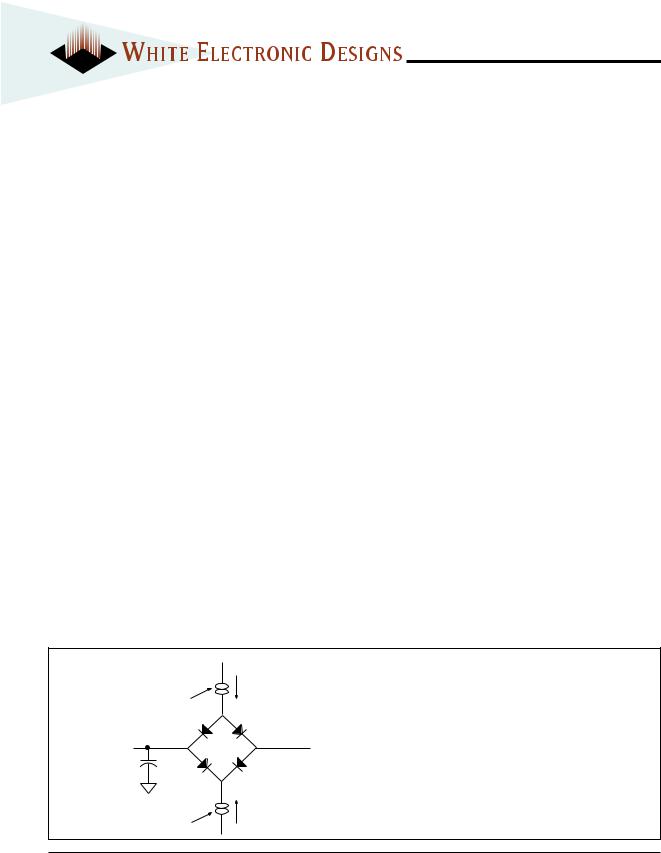
FIG. 2
AC TEST CIRCUIT
I OL
Current Source
D.U.T. |
VZ ≈1.5V |
Ceff = 50 pf |
(Bipolar Supply) |
|
IOH
Current Source
AC TEST CONDITIONS
Parameter |
Typ |
Unit |
Input Pulse Levels |
VIL = 0, VIH = 3.0 |
V |
|
|
|
Input Rise and Fall |
5 |
ns |
|
|
|
Input and Output Reference Level |
1.5 |
V |
|
|
|
Output Timing Reference Level |
1.5 |
V |
|
|
|
NOTES:
VZ is programmable from -2V to +7V. IOL & IOH programmable from 0 to 16mA. Tester Impedance Z0 = 75 Ω.
VZ is typically the midpoint of VOH and VOL.
IOL & IOH are adjusted to simulate a typical resistive load circuit. ATE tester includes jig capacitance.
White Electronic Designs Corporation • Phoenix, AZ • (602) 437-1520 |
2 |

WRITE
A write cycle is initiated when OE is high and a low pulse is on WE or CS with CS or WE low. The address is latched on the falling edge of CS or WE whichever occurs last. The data is latched by the rising edge of CS or WE, whichever occurs first. A word write operation will automatically continue to completion.
WRITE CYCLE TIMING
Figures 3 and 4 show the write cycle timing relationships. A write cycle begins with address application, write enable and chip select. Chip select is accomplished by placing the CS line low. Write enable consists of setting the WE line low. The write cycle begins when the last of either CS or WE goes low.
The WE line transition from high to low also initiates an internal 150 sec delay timer to permit page mode operation. Each subsequent WE transition from high to low that occurs before the completion of the 150 sec time out will restart the timer from zero. The operation of the timer is the same as a retriggerable one-shot.
WE512K16-XG4X
AC WRITE CHARACTERISTICS
(VCC = 5.0V, GND = 0V, TA = -55°C to +125°C)
Write Cycle Parameter |
Symbol |
Min |
Max |
Unit |
||||
Write Cycle Time, TYP = 6ms |
tWC |
|
10 |
ms |
||||
Address Set-up Time |
tAS |
10 |
|
ns |
||||
|
|
|
|
|
|
|
||
Write Pulse Width |
(WE |
or |
CS) |
|
tWP |
120 |
|
ns |
Chip Select Set-up Time |
tCS |
0 |
|
ns |
||||
Address Hold Time |
tAH |
100 |
|
ns |
||||
Data Hold Time |
tDH |
10 |
|
ns |
||||
Chip Select Hold Time |
tCSH |
0 |
|
ns |
||||
Data Set-up Time |
tDS |
100 |
|
ns |
||||
Output Enable Set-up Time |
tOES |
10 |
|
ns |
||||
Output Enable Hold Time |
tOEH |
10 |
|
ns |
||||
Write Pulse Width High |
tWPH |
50 |
|
ns |
||||
3 |
White Electronic Designs Corporation • Phoenix, AZ • (602) 437-1520 |
 Loading...