


EDI88512LPA55NC
White Electronic Designs EDI88512LPA55NC, EDI88512LPA55NB, EDI88512LPA55N36M, EDI88512LPA55N36I, EDI88512LPA55N36C Datasheet
...
1 White Electronic Designs Corporation • (602) 437-1520 • www.whiteedc.com
EDI88512CA
512Kx8 Monolithic SRAM, SMD 5962-95600
FEATURES
■ Access Times of 15, 17, 20, 25, 35, 45, 55ns
■ Data Retention Function (LPA version)
■ TTL Compatible Inputs and Outputs
■ Fully Static, No Clocks
■ Organized as 512Kx8
■ Commercial, Industrial and Military Temperature Ranges
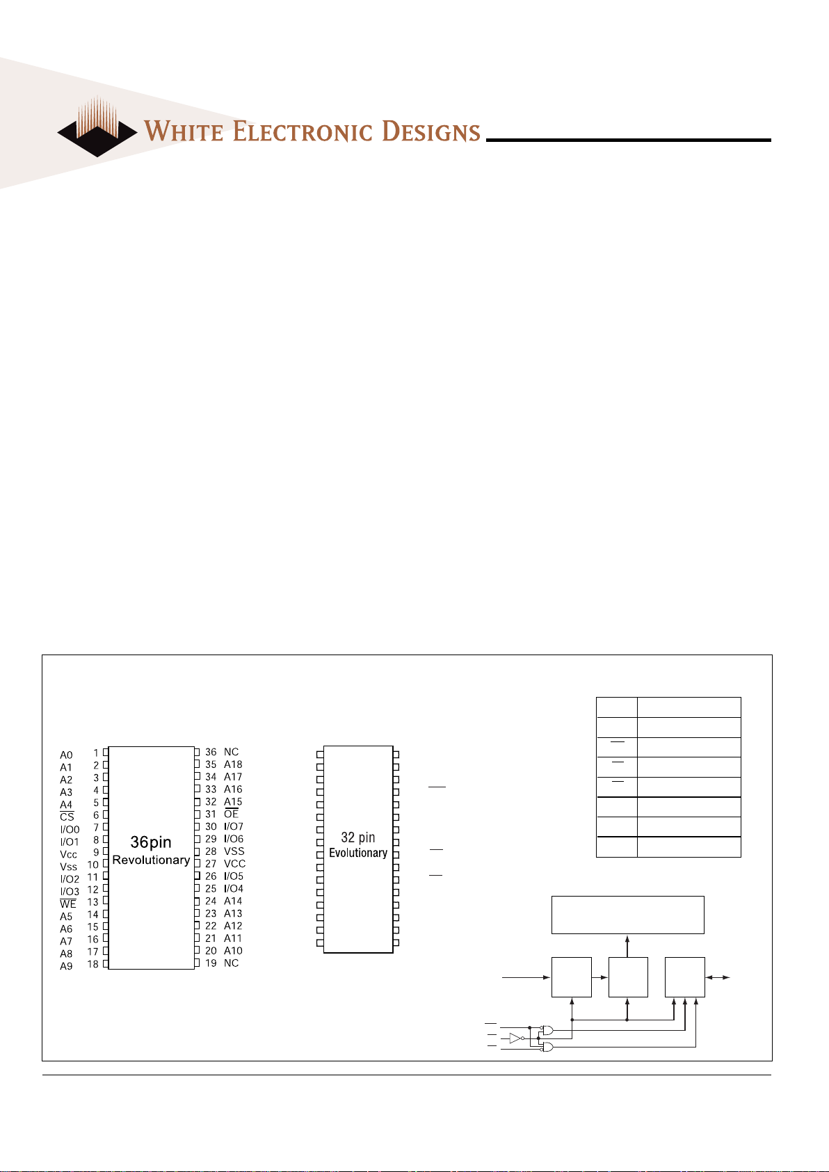
■ 32 lead JEDEC Approved Evolutionary Pinout
• Ceramic Sidebrazed 600 mil DIP (Package 9)
• Ceramic Sidebrazed 400 mil DIP (Package 326)
• Ceramic 32 pin Flatpack (Package 344)
• Ceramic Thin Flatpack (Package 321)
• Ceramic SOJ (Package 140)
■ 36 lead JEDEC Approved Revolutionary Pinout
• Ceramic Flatpack (Package 316)
• Ceramic SOJ (Package 327)
• Ceramic LCC (Package 502)
■ Single +5V (±10%) Supply Operation
The EDI88512CA is a 4 megabit Monolithic CMOS
Static RAM.
The 32 pin DIP pinout adheres to the JEDEC evolu-
tionary standard for the four megabit device. All 32 pin
packages are pin for pin upgrades for the single chip
enable 128K x 8, the EDI88128CS. Pins 1 and 30 be-
come the higher order addresses.
The 36 pin revolutionary pinout also adheres to the
JEDEC standard for the four megabit device. The cen-
ter pin power and ground pins help to reduce noise in
high performance systems. The 36 pin pinout also
allows the user an upgrade path to the future 2Mx8.
A Low Power version with Data Retention
(EDI88512LPA) is also available for battery backed
applications. Military product is available compliant to
Appendix A of MIL-PRF-38535.
36 PIN
TOP VIEW
PIN DESCRIPTION
I/O0-7 Data Inputs/Outputs
A0-18 Address Inputs
WE Write Enables
CS Chip Selects
OE Output Enable
VCC Power (+5V ±10%)
VSS Ground
NC Not Connected
BLOCK DIAGRAM
Memory Array
Address
Buffer
Address
Decoder
I/O
Circuits
A
-18
I/O
-7
WE
CS
OE
FIG. 1 PIN CONFIGURATION
32 PIN
TOP VIEW
32
31
30
29
28
27
26
25
24
23
22
21
20
19
18
17
1
2
3
4
5
6
7
8
9
10
11
12
13
14
15
16
V
CC
A15
A17
WE
A13
A8
A9
A11
OE
A10
CS
I/O7
I/O6
I/O5
I/O4
I/O3
A18
A16
A14
A12
A7
A6
A5
A4
A3
A2
A1
A0
I/O0
I/O1
I/O2
V
SS
Aug. 2002 Rev. 9

2
White Electronic Designs Corporation • Phoenix AZ • (602) 437-1520
EDI88512CA
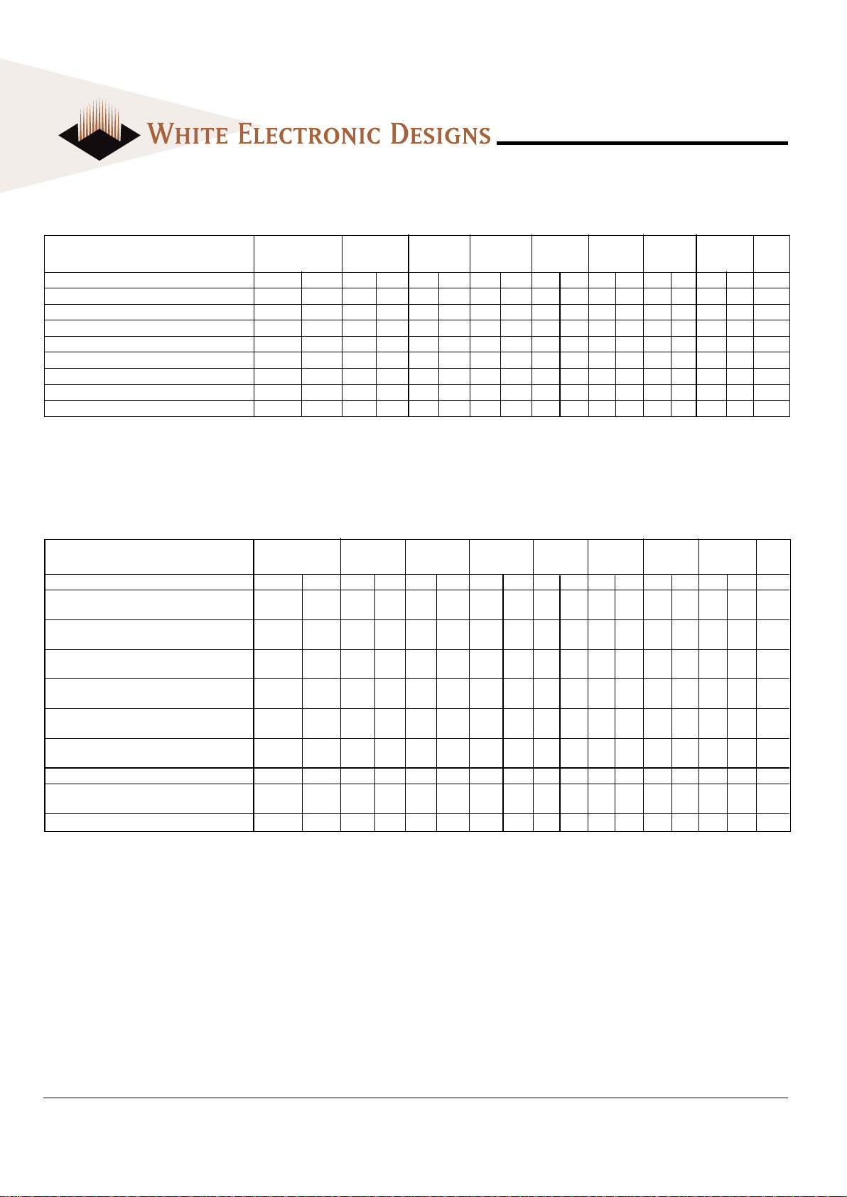
ABSOLUTE MAXIMUM R ATINGS
Parameter Unit
Voltage on any pin relative to Vss -0.5 to 7.0 V
Operating Temperature TA (Ambient)
Commercial 0 to +70 °C
Industrial -40 to +85 °C
Military -55 to +125 °C
Storage Temperature, Plastic -65 to +150 °C
Power Dissipation 1.5 W
Output Current 20 mA
Junction Temperature, T
J 175 °C
RECOMMENDED OPERATING CONDITIONS
Parameter Symbol Min Typ Max Unit
Supply Voltage VCC 4.5 5.0 5.5 V
Supply Voltage VSS 00 0V
Input High Voltage VIH 2.2 — 3.0 V
Input Low Voltage V
IL -0.3 — +0.8 V
Parameter Symbol Condition Max Unit
Address Lines CI VIN = Vcc or Vss, f = 1.0MHz 12 pF
Data Lines C
O VOUT = Vcc or Vss, f = 1.0MHz 14 pF
These parameters are sampled, not 100% tested.
CAPACITANCE
(TA = +25°C)
TRUTH TABLE
OE CS WE Mode Output Power
X H X Standby High Z Icc2 , Icc3
H L H Output Deselect High Z Icc1
L L H Read Data Out Icc1
X L L Write Data In Icc1
NOTE:
Stress greater than those listed under "Absolute Maximum Ratings"
may cause permanent damage to the device. This is a stress rating
only and functional operation of the device at these or any other
conditions greater than those indicated in the operational sections of
this specification is not implied. Exposure to absolute maximum
rating conditions for extended periods may affect reliability.
Input Pulse Levels VSS to 3.0V
Input Rise and Fall Times 5ns
Input and Output Timing Levels 1.5V
Output Load Figure 1
NOTE: For t
EHQZ, tGHQZ and tWLQZ, CL = 5pF Figure 2)
30pF
480Ω
Vcc
Q
Figure 1 Figure 2
255Ω
5pF
480Ω
Vcc
Q
255Ω
AC TEST CONDITIONS
Parameter Symbol Conditions Units
Min Max
Input Leakage Current ILI VIN = 0V to VCC -10 10 µA
Output Leakage Current ILO VI/O = 0V to VCC -10 10 µA
Operating Power Supply Current ICC1 WE, CS = VIL, II /O = 0mA, Min Cycle (17ns) — 250 mA
(20 -55ns) — 225 mA
Standby (TTL) Power Supply Current ICC2 CS ³ VIH, VIN £ VIL, VIN ³ VIH —60mA
Full Standby Power Supply Current ICC3 CS ³ VCC -0.2V CA — 25 mA
VIN ³ Vcc -0.2V or VIN £ 0.2V LPA — 20 mA
Output Low Voltage VOL IOL = 8.0mA — 0.4 V
Output High Voltage V
OH IOH = -4.0mA 2.4 — V
NOTE: DC test conditions: V
IL = 0.3V, VIH = Vcc -0.3V
DC CHARACTERISTICS
(VCC
= 5V, TA = -55°C TO +125°C)
3 White Electronic Designs Corporation • (602) 437-1520 • www.whiteedc.com
EDI88512CA
AC CHARACTERISTICS – READ CYCLE
(VCC
= 5.0V, VSS = 0V, TA
= -55°C TO +125°C)
Symbol 15ns 17ns 20ns 25ns 35ns 45ns 55ns
Parameter JEDEC Alt. Min Max Min Max Min Max Mi n Max Min Max Min Max Min Max Units
Read Cycle Time tAVAV tRC 15 17 20 25 35 45 55 ns
Address Access Time tAVQV tAA 15 17 20 25 35 45 55 ns
Chip Enable Access Time tELQV tACS 15 17 20 25 35 45 55 n s
Chip Enable to Output in Low Z (1) tELQX tCLZ 2333333ns
Chip Disable to Output in High Z (1) tEHQZ tCHZ 07 07 08 010015020020ns
Output Hold from Address Change tAVQX tOH 0000000ns
Output Enable to Output Valid tGLQV tOE 8 8 10 12 15 25 30 ns
Output Enable to Output in Low Z (1) tGLQX tOLZ 0000000ns
Output Disable to Output in High Z(1) t
GHQZ tOHZ 07 07 08 010015020020ns
1. This parameter is guaranteed by design but not tested.
AC CHARACTERISTICS – WRITE CYCLE
(VCC
= 5.0V, VSS = 0V, TA
= -55°C TO +125°C)
Symbol 15ns 17ns 20ns 25ns 35ns 45ns 55ns
Parameter JEDEC Alt. Min Max Min Max Min Max Min Max Min Max Min Max Min Max Units
Write Cycle Time tAVAV tWC 15 17 20 25 35 45 55 ns
Chip Enable to End of Write t
ELWH tCW 13 14 15 17 25 30 50 ns
tELEH tCW 13 14 15 17 25 30 50 ns
Address Setup Time t
AVWL tAS 00 00000ns
tAVEL tAS 00 00000ns
Address Valid to End of Write t
AVWH tAW 13 14 15 17 25 30 50 n s
tAVEH tAW 13 14 15 17 25 30 50 ns
Write Pulse Width t
WLWH t WP 13 14 15 17 25 30 45 ns
tWLEH tWP 13 14 15 17 25 30 45 ns
Write Recovery Time t
WHAX tWR 00 00000ns
tEHAX t WR 00 00000ns
Data Hold Time t
WHDX tDH 00 00000ns
tEHDX t DH 00 00000ns
Write to Output in High Z (1) tWLQZ tWHZ 080808010025030030ns
Data to Write Time t
DVWH tDW 8 8 10 12 20 25 40 ns
tDVEH t DW 8 8 10 12 20 25 30 ns
Output Active from End of Write (1) t
WHQX tWLZ 00 00000ns
1. This parameter is guaranteed by design but not tested.
 Loading...