


WS1M8V-55CMA
White Electronic Designs WS1M8V-55CMA, WS1M8V-55CM, WS1M8V-55CI, WS1M8V-55CIA, WS1M8V-55CCA Datasheet
...
1
White Microelectronics • Phoenix, AZ • (602) 437-1520
3
SRAM DUALITHICS
2x512Kx8 DUALITHIC™ SRAM
ADVANCED*
WS1M8V-XCX
FEATURES
■ Access Times 17, 20, 25, 35, 45, 55ns
■ Evolutionary, Corner Power/Ground Pinout
■ Packaging:
•32 pin, Hermetic Ceramic DIP (Package 300)
■ Organized as two banks of 512Kx8
■ Commercial, Industrial and Military Temperature Ranges
■ 3.3V Power Supply
■ Low Power CMOS
■ TTL Compatible Inputs and Outputs
■ Output Enable Internally tied to GND.
* This data sheet describes a product that may or may not be under
development and is subject to change or cancellation without notice.
October 1998
NOTE:
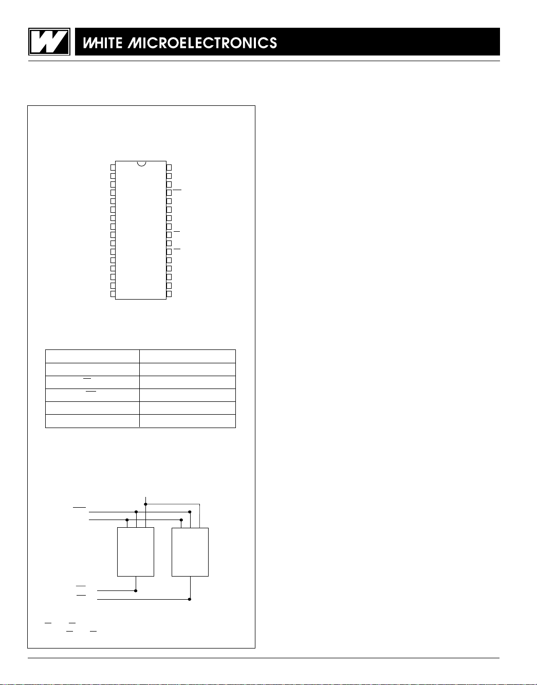
1. CS
1 and CS2 are used to select the lower and upper 512Kx8 of the
device. CS1 and CS2 must not be enabled at the same time.
1
2
3
4
5
6
7
8
9
10
11
12
13
14
15
16
32
31
30
29
28
27
26
25
24
23
22
21
20
19
18
17
A18
A16
A14
A12
A7
A6
A5
A4
A3
A2
A1
A0
I/O0
I/O1
I/O2
GND
V
CC
A15
A17
WE
A13
A8
A9
A11
CS2
A10
CS1
I/O7
I/O6
I/O5
I/O4
I/O3
PIN CONFIGURATION FOR WS1M8V-XCX
32 DIP
TOP VIEW
BLOCK DIAGRAM
512K x 8
512K x 8
A
0-18
WE
CS
1
CS
2
I/O
0-7
(1)
(1)
A0-18 Address Inputs
I/O0-7 Data Input/Output
CS1-2 Chip Selects
WE Write Enable
VCC +3.3V Power Supply
GND Ground
PIN DESCRIPTION
2
White Microelectronics • Phoenix, AZ • (602) 437-1520
3
SRAM DUALITHICS
WS1M8V-XCX
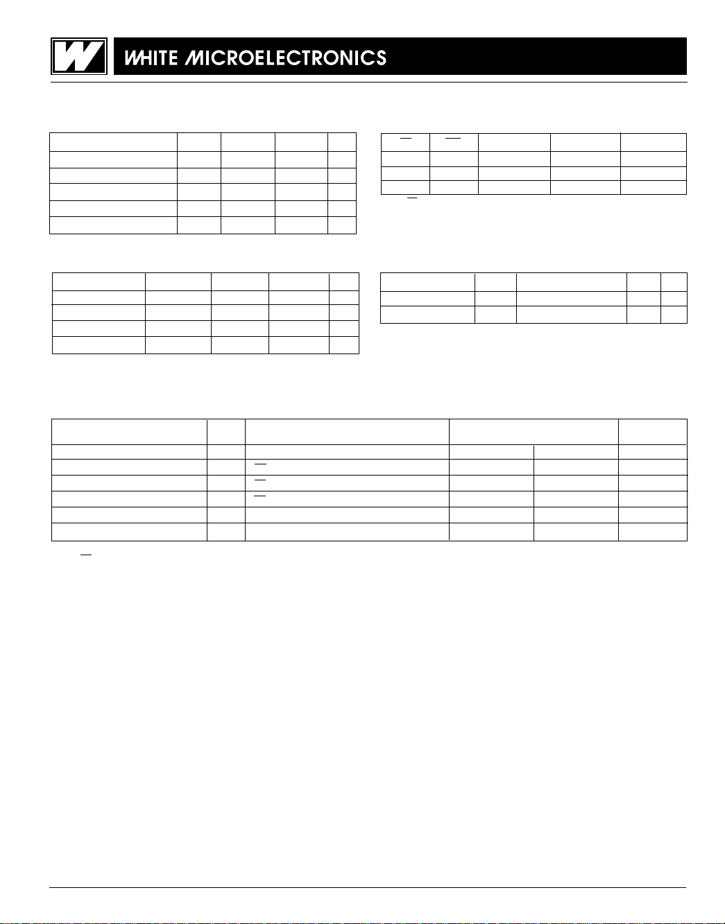
TRUTH TABLEABSOLUTE MAXIMUM RATINGS
Parameter Symbol Min Max Unit
Operating Temperature T
A -55 +125 °C
Storage Temperature T
STG -65 +150 °C
Signal Voltage Relative to GND V
G -0.5 +4.6 V
Junction Temperature T
J 150 °C
Supply Voltage V
CC -0.5 5.5 V
CS WE Mode Data I/O Power
H X Standby High Z Standby
L H Read Data Out Active
L L Write Data In Active
NOTE: OE is internally tied to GND.
RECOMMENDED OPERATING CONDITIONS
Parameter
Symbol
Condition Max Unit
Input capacitance CIN
V
IN
= 0V, f = 1.0MHz
28 pF
Output capicitance C
OUT
V
OUT
= 0V, f = 1.0MHz
28 pF
This parameter is guaranteed by design but not tested.
Parameter Symbol Min Max Unit
Supply Voltage V
CC 3.0 3.6 V
Input High Voltage V
IH 2.2 VCC + 0.3 V
Input Low Voltage V
IL -0.3 +0.8 V
Operating Temp. (Mil.) T
A -55 +125 °C
CAPACITANCE
(T
A = +25°C)
DC CHARACTERISTICS
(V
CC
= 3.3V, GND = 0V, TA = -55°C to +125°C)
Parameter Sym Conditions Units
Min Max
Input Leakage Current ILI VCC = 3.6, VIN = GND to VCC 10 µA
Output Leakage Current ILO
1
CS = VIH, VOUT = GND to VCC 10 µA
Operating Supply Current ICC
1
CS = VIL, f = 5MHz, Vcc = 3.6 160 mA
Standby Current ISB
1
CS = VIH, f = 5MHz, Vcc = 3.6 30 mA
Output Low Voltage VOL IOL = 8.0mA 0.4 V
Output High Voltage V
OH IOH = -4.0mA 2.4 V
NOTE: DC test conditions: VIH = VCC -0.3V , VIL = 0.3V
1. OE is internally tied to GND.
 Loading...