


White Electronic Designs EDI8L3265C25AC, EDI8L3265C20AI, EDI8L3265C20AC, EDI8L3265C15AI, EDI8L3265C15AC Datasheet
...
|
|
|
EDI8L3265C |
|
|
|
|
64Kx32 SRAM |
|
Features |
64Kx32CMOSHighSpeed |
|||
64Kx32 bit CMOS Static |
Static RAM |
|||
|
|
|||
RandomNOTAccess Memory Array |
The EDI8L3265C is a high speed, high performance, four |
|||
• |
Fast Access Times: 12*, 15, 20, and 25ns |
megabit density Static RAM organized as a 64Kx32 bit |
||
array. |
||||
• |
Individual Byte Selects |
|||
Four Byte Selects, two Chip Enables, Write Control, and |
||||
• |
User Configurable Organization |
Output Enable provide the user with a flexible memory |
||
|
with Minimal Additional Logic |
solution. The user may independently enable each of the |
||
|
four bytes, and, with minimal additional peripheral logic, |
|||
• |
Master Output Enable and Write Control |
|||
the unit may be configured as a 128Kx16 array. |
||||
• |
TTL Compatible Inputs and Outputs |
|||
Fully asynchronous circuitry is used, requiring no clocks or |
||||
• Fully Static, No Clocks |
refreshing for operation and providing equal access and |
|||
Surface Mount Package |
cycle times for ease of use. |
|||
The EDI8L3265C, allows 2 megabits of memory to be |
||||
• |
68 Lead PLCC, No. 99 (JEDEC-M0-47AE) |
|||
placed in less than 0.990 square inches of board space. |
||||
• Small Footprint, 0.990 Sq. In. |
||||
The EDI8L3265C can be upgraded to 128K, 256K or |
||||
• |
Multiple Ground Pins for Maximum |
512Kx32 in the same footprint using the EDI8L32128, |
||
|
Noise Immunity |
EDI8L32256 or the EDI8L32512C. (See page 6 for up- |
||
|
grade paths). |
|||
Single +5V (±5%) Supply Operation |
||||
|
|
|||
|
RECOMMENDEDNote: Solder Reflow temperatures should not exceed 260°C for 10 seconds. |
|||
*AdvanceInformation |
|
|
||
Pin Configurations and Block Diagram
Notes:1.Seepage6forupgradepaths.
PinNames
AØ-A15 |
|
Address Inputs |
|||||||
EØ-E1 |
|
Chip Enables (one per word) |
|||||||
|
|
|
|
|
|
|
|
|
|
BSØ-BS3 |
|
Byte Selects (One per Byte) |
|||||||
FOR |
|||||||||
W |
|
Master Write Enable |
|||||||
G |
|
Master Output Enable |
|||||||
DQØ-DQ31 |
|
CommonDataInput/Output |
|||||||
VCC |
|
Power (+5V±5%) |
|||||||
VSS |
|
Ground |
|||||||
NC |
|
No Connection |
|||||||
|
|
|
|
|
|
|
|
NEW |
|
|
|
|
|
|
|
|
|
|
|
|
|
|
|
|
|
|
|
|
|
|
|
|
|
|
|
|
|
|
|
|
|
|
|
|
|
|
|
|
|
|
|
|
|
|
|
|
|
|
|
|
|
|
|
|
|
|
|
|
|
DESIGN
March 1997 Rev. 4 |
1 |
White Electronic Designs Corporation • (602) 437-1520 • www.whiteedc.com |
ECO#8302 |
|
|
EDI8L3265C
64Kx32 SRAM
AbsoluteMaximumRatings*
Voltage on any pin relative to VSS |
-0.5V to 7.0V |
Operating Temperature TA (Ambient) |
|
Commercial |
0°C to + 70°C |
Industrial |
-40°C to +85°C |
Storage Temperature |
-55°C to +125°C |
Power Dissipation |
3.0 Watts |
Output Current. |
20 mA |
Junction Temperature, TJ |
175°C |
|
|
*Stressgreaterthanthoselistedunder"AbsoluteMaximumRatings"maycausepermanent damagetothedevice. Thisisastressrating onlyandfunctionaloperationofthedeviceat theseoranyotherconditionsgreaterthanthoseindicatedintheoperationalsectionsofthis specificationisnotimplied. Exposuretoabsolutemaximumratingconditionsforextended periodsmayaffectreliability.
DCElectricalCharacteristics
RecommendedDCOperatingConditions
Parameter |
Sym |
Min |
Typ |
Max |
Units |
Supply Voltage |
VCC |
4.75 |
5.0 |
5.25 |
V |
Supply Voltage |
VSS |
0 |
0 |
0 |
V |
Input High Voltage |
VIH |
2.2 |
-- |
VCC+0.5 |
V |
Input Low Voltage |
VIL |
-0.3 |
-- |
0.8 |
V |
|
|
|
|
|
|
ACTestConditions
Input Pulse Levels |
VSS to 3.0V |
|
|
Input Rise and Fall Times |
5ns |
Input and Output Timing Levels |
1.5V |
Output Load |
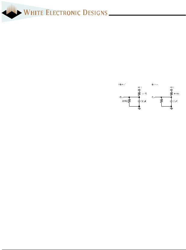
Figure 1 |
|
|
(note: For TEHQZ,TGHQZ and TWLQZ, CL = 5pF)
Parameter |
Sym |
|
|
|
|
|
Conditions |
Min |
Max |
|
Unit |
|
|
|
|
|
|
|
|
12ns* 15ns |
20/25ns |
ns |
|
Operating Power |
ICC1 |
|
|
|
|
|
|
500 |
460 |
420 |
mA |
|
W= VIL, II/O = 0mA, |
||||||||||
Supply Current |
|
|
|
|
|
Min Cycle |
|
|
|
|
|
Standby (TTL) |
ICC2 |
|
|
³ VIH, VIN £ VIL or |
60 |
60 |
60 |
mA |
|||
E |
|||||||||||
Supply Current |
|
|
VIN ³ VIH, f=ØMHz |
|
|
|
|
||||
Full Standby |
ICC3 |
|
|
|
|
|
³ VCC-0.2V |
20 |
20 |
20 |
mA |
|
|
|
E |
||||||||
Supply Current CMOS |
|
VIN ³ VCC-0.2V or VIN £ 0.2V |
|
|
|
|
|||||
Input Leakage Current |
ILI |
|
|
VIN = 0V to VCC |
±10 |
±10 |
±10 |
µA |
|||
Output Leakage Current |
ILO |
|
|
V I/O = 0V to VCC |
±10 |
±10 |
±10 |
µA |
|||
Output High Volltage |
VOH |
|
|
|
|
IOH = -4.0mA |
2.4 |
|
|
V |
|
Output Low Voltage |
VOL |
|
|
|
|
IOL = 8.0mA |
0.4 |
0.4 |
0.4 |
V |
|
|
|
|
|
|
|
|
|
|
|
|
|
*Typical: TA = 25°C, VCC = 5.0V *AdvancedInformation
TruthTable |
|
|
|
|
|
Capacitance |
|
|
|
|
|
|
||||||||
|
|
|
|
|
|
|
|
|
|
|
|
|
|
(f=1.0MHz,VIN=VCCorVSS) |
|
|
||||
E W G BSØ-3 |
Mode |
Output |
Power |
|
|
|
||||||||||||||
|
|
|
|
|
|
|
|
|||||||||||||
H |
X |
|
X |
|
X |
Standby |
High Z |
ICC2,ICC3 |
|
|
Parameter |
Sym |
Max |
Unit |
||||||
L |
H |
|
H |
|
X |
Output Disable |
High Z |
ICC1 |
|
|
||||||||||
|
|
|
Address Lines |
CA |
20 |
pF |
||||||||||||||
L |
X |
|
X |
|
H |
Output Disable |
High Z |
ICC1 |
|
|
||||||||||
|
|
|
Data Lines |
CD/Q |
10 |
pF |
||||||||||||||
L |
H |
|
L |
|
L |
Read |
Dout |
ICC1 |
|
|
||||||||||
|
|
|
|
|
|
|
|
|
|
|||||||||||
|
Write & Output |
W, G |
16 |
pF |
||||||||||||||||
L |
L |
|
X |
|
L |
Write |
Din |
ICC1 |
|
|||||||||||
|
|
|
Enable Lines |
|
|
|
|
|
bF |
|||||||||||
X Means Don't Care |
|
|
|
|
|
|
|
|
|
|
||||||||||
|
|
|
|
|
|
|
|
|
|
|
|
|||||||||
|
|
|
|
|
Chip Enable Lines |
E, BS |
9 |
pF |
||||||||||||
|
|
|
|
|
|
|
|
|
|
|
|
|
|
|||||||
|
|
|
|
|
|
|
|
|
|
|
|
|
|
|
|
|
|
|
|
|
Theseparametersaresampled,not100%tested.
White Electronic Designs Corporation • (602) 437-1520 • www.whiteedc.com |
2 |
 Loading...