


Texas Instruments CD4066BPW, CD4066BNSR, CD4066BM96, CD4066BM, CD4066BF3A Datasheet
...CD4066B CMOS QUAD BILATERAL SWITCH
SCHS051C – REVISED FEBRUARY 2003
D15-V Digital or ± 7.5-V Peak-to-Peak
Switching
D125-Ω Typical On-State Resistance for 15-V
Operation
DSwitch On-State Resistance Matched to Within 5 Ω Over 15-V Signal-Input Range
DOn-State Resistance Flat Over Full Peak-to-Peak Signal Range
DHigh On/Off Output-Voltage Ratio: 80 dB Typical at fis = 10 kHz, RL = 1 kΩ
DHigh Degree of Linearity: <0.5% Distortion
Typical at fis = 1 kHz, Vis = 5 V p-p, VDD – VSS ≥ 10 V, RL = 10 kΩ
DExtremely Low Off-State Switch Leakage, Resulting in Very Low Offset Current and
High Effective Off-State Resistance: 10 pA Typical at VDD – VSS = 10 V, TA = 25° C
DExtremely High Control Input Impedance
(Control Circuit Isolated From Signal Circuit): 1012 Ω Typical
DLow Crosstalk Between Switches: –50 dB Typical at fis = 8 MHz, RL = 1 kΩ
DMatched Control-Input to Signal-Output Capacitance: Reduces Output Signal Transients
DFrequency Response, Switch On = 40 MHz Typical
D100% Tested for Quiescent Current at 20 V
D5-V, 10-V, and 15-V Parametric Ratings
DMeets All Requirements of JEDEC Tentative Standard No. 13B, Standard Specifications for Description of B-Series CMOS Devices
DApplications:
–Analog Signal Switching/Multiplexing: Signal Gating, Modulator, Squelch Control, Demodulator, Chopper, Commutating Switch
–Digital Signal Switching/Multiplexing
–Transmission-Gate Logic Implementation
–Analog-to-Digital and Digital-to-Analog Conversion
–Digital Control of Frequency, Impedance, Phase, and Analog-Signal Gain
E, F, M, NS, OR PW PACKAGE
|
|
(TOP VIEW) |
|
||
SIG A IN/OUT |
|
|
|
|
VDD |
|
1 |
14 |
|
||
|
|
||||
SIG A OUT/IN |
|
|
|
|
|
|
2 |
13 |
|
CONTROL A |
|
SIG B OUT/IN |
|
3 |
12 |
|
CONTROL D |
|
|
||||
SIG B IN/OUT |
|
4 |
11 |
|
SIG D IN/OUT |
|
|
||||
CONTROL B |
|
5 |
10 |
|
SIG D OUT/IN |
|
|
||||
CONTROL C |
|
6 |
9 |
|
SIG C OUT/IN |
|
|
||||
VSS |
|
7 |
8 |
|
SIG C IN/OUT |
|
|
||||
|
|
|
|
|
|
description/ordering information
ORDERING INFORMATION
T |
PACKAGE† |
ORDERABLE |
TOP-SIDE |
||
|
|
||||
A |
|
|
PART NUMBER |
MARKING |
|
|
|
|
|||
|
CDIP – F |
Tube |
CD4066BF3A |
CD4066BF3A |
|
|
|
|
|
|
|
|
PDIP – E |
Tube |
CD4066BE |
CD4066BE |
|
|
|
|
|
|
|
|
SOIC – M |
Tube |
CD4066BM |
CD4066BM |
|
–55° C to 125° C |
|
|
|||
Tape and reel |
CD4066BM96 |
||||
|
|
||||
|
|
|
|
|
|
|
SOP – NS |
Tape and reel |
CD4066BNSR |
CD4066B |
|
|
|
|
|
|
|
|
TSSOP – PW |
Tube |
CD4066BPW |
CM066B |
|
|
|
|
|||
|
Tape and reel |
CD4066BPWR |
|||
|
|
|
|||
|
|
|
|
|
|
†Package drawings, standard packing quantities, thermal data, symbolization, and PCB design guidelines are available at www.ti.com/sc/package.
Please be aware that an important notice concerning availability, standard warranty, and use in critical applications of Texas Instruments semiconductor products and disclaimers thereto appears at the end of this data sheet.
PRODUCTION DATA information is current as of publication date. Products conform to specifications per the terms of Texas Instruments standard warranty. Production processing does not necessarily include testing of all parameters.
Copyright 2003, Texas Instruments Incorporated
POST OFFICE BOX 655303 • DALLAS, TEXAS 75265 |
1 |
CD4066B
CMOS QUAD BILATERAL SWITCH
SCHS051C – REVISED FEBRUARY 2003
description/ordering information (continued)
CD4066B is a quad bilateral switch intended for the transmission or multiplexing of analog or digital signals. It is pin-for-pin compatible with the CD4016B, but exhibits a much lower on-state resistance. In addition, the on-state resistance is relatively constant over the full input-signal range.
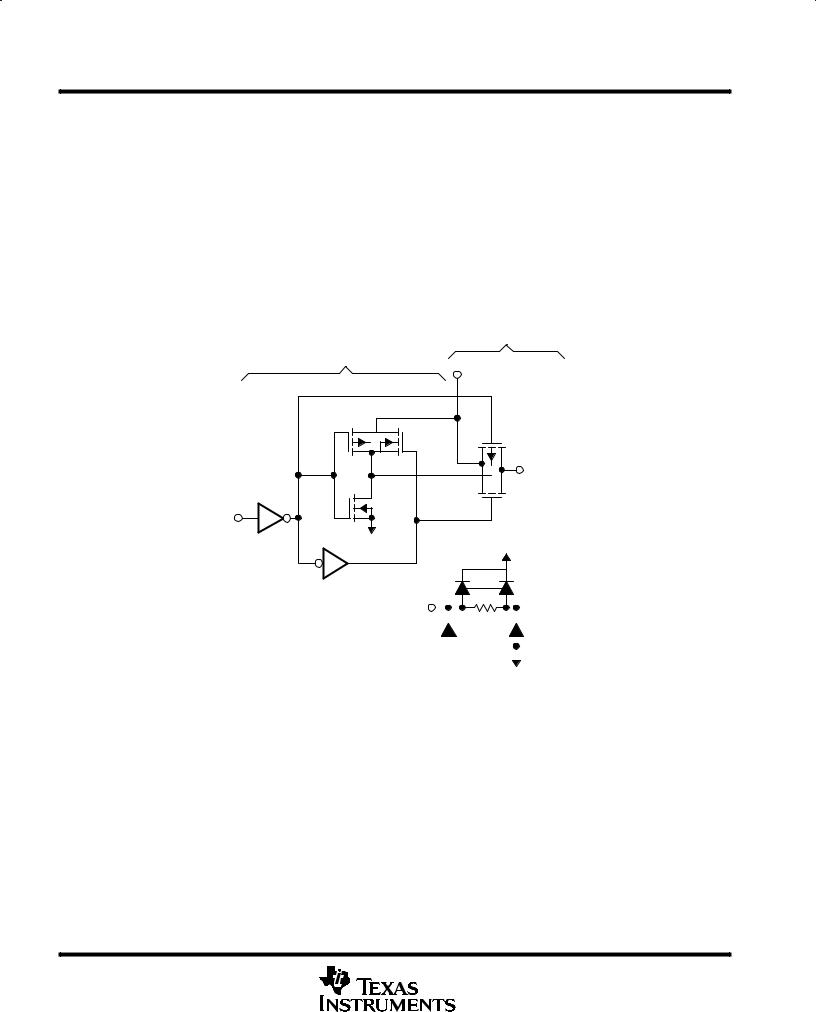
The CD4066B consists of four bilateral switches, each with independent controls. Both the p and the n devices in a given switch are biased on or off simultaneously by the control signal. As shown in Figure 1, the well of the n-channel device on each switch is tied to either the input, when the switch is on, or to VSS when the switch is off. This configuration eliminates the variation of the switch-transistor threshold voltage with input signal and, thus, keeps the on-state resistance low over the full operating-signal range.
The advantages over single-channel switches include peak input-signal voltage swings equal to the full supply voltage and more constant on-state impedance over the input-signal range. However, for sample-and-hold applications, the CD4016B is recommended.
Switch
Control
IN
Vis
p  n
n
p
OUT
 n Vos
n Vos
CONTROL |
n |
|
V |
† |
|
|
C |
|
|
|
VSS |
VDD
|
|
|
|
|
|
|
|
|
|
|
|
VSS |
|
|
|
|
|
|
|
|
|
|
|
|
|
|
|
|
|
|
|
|
|
|
|
|
|
|
|
|
|
|
|
|
|
|
|
|
|
|
|
|
|
||
† All control inputs are protected by CMOS protection network. |
|
||||||||||||
NOTES: A. All p substrates are connected to VDD. |
|
||||||||||||
B. |
Normal operation control-line biasing: Switch on (logic 1), VC = VDD; Switch off (logic 0), VC = VSS |
|
|||||||||||
C. |
Signal-level range: VSS ≤ Vis ≤ VDD |
92CS - 29113 |
|||||||||||
Figure 1. Schematic Diagram of One-of-Four Identical Switches and Associated Control Circuitry
2 |
POST OFFICE BOX 655303 • DALLAS, TEXAS 75265 |

CD4066B
CMOS QUAD BILATERAL SWITCH
SCHS051C – REVISED FEBRUARY 2003
absolute maximum ratings over operating free-air temperature (unless otherwise noted)†
DC supply-voltage range, (VDD) (voltages referenced to VSS terminal) . . . . . . . . . . . . |
. . . . . . –0.5 V to 20 V |
|
Input voltage range, Vis, all inputs . . . . . . . . . . . . . . . . . . . . . . . . . . . . . . . . . . . . . . . . . . . . . |
–0.5 V to VDD + |
0.5 V |
DC input current, IIN, any one input . . . . . . . . . . . . . . . . . . . . . . . . . . . . . . . . . . . . . . . . . . . . |
. . . . . . . . . . . ± |
10 mA |
Package thermal impedance, θ JA (see Note 1): E package . . . . . . . . . . . . . . . . . . . . . . . . |
. . . . . . . . . . . 80° C/W |
|
M package . . . . . . . . . . . . . . . . . . . . . . . |
. . . . . . . . . . . 86° C/W |
|
NS package . . . . . . . . . . . . . . . . . . . . . . |
. . . . . . . . . . . 76° C/W |
|
PW package . . . . . . . . . . . . . . . . . . . . . . |
. . . . . . . . . . 113° C/W |
|
Lead temperature (during soldering): |
|
|
At distance 1/16 ± 1/32 inch (1,59 ± 0,79 mm) from case for 10 s max . . . . . . . . . . . |
. . . . . . . . . . . . |
265° C |
Storage temperature range, Tstg . . . . . . . . . . . . . . . . . . . . . . . . . . . . . . . . . . . . . . . . . . . . . . . |
. . . . –65° C to 150° C |
|
†Stresses beyond those listed under “absolute maximum ratings” may cause permanent damage to the device. These are stress ratings only, and functional operation of the device at these or any other conditions beyond those indicated under “recommended operating conditions” is not implied. Exposure to absolute-maximum-rated conditions for extended periods may affect device reliability.
NOTE 1: The package thermal impedance is calculated in accordance with JESD 51-7.
recommended operating conditions
|
|
MIN |
MAX |
UNIT |
|
|
|
|
|
VDD |
Supply voltage |
3 |
18 |
V |
TA |
Operating free-air temperature |
–55 |
125 |
° C |
POST OFFICE BOX 655303 • DALLAS, TEXAS 75265 |
3 |

CD4066B
CMOS QUAD BILATERAL SWITCH
SCHS051C – REVISED FEBRUARY 2003
electrical characteristics
|
|
|
|
|
|
|
|
LIMITS AT INDICATED TEMPERATURES |
|
|||||
|
|
|
|
|
|
|
|
|
|
|
|
|
|
|
|
PARAMETER |
TEST CONDITIONS |
|
VIN |
VDD |
° |
° |
° |
125° C |
25° C |
UNIT |
|||
|
|
|
|
|
|
(V) |
(V) |
–55 C |
–40 C |
85 C |
|
TYP |
MAX |
|
|
|
|
|
|
|
|
|
|
|
|
||||
|
|
|
|
|
|
|
|
|
|
|
|
|
|
|
|
|
|
|
|
|
0, 5 |
5 |
0.25 |
0.25 |
7.5 |
7.5 |
0.01 |
0.25 |
|
|
|
|
|
|
|
|
|
|
|
|
|
|
|
|
IDD |
Quiescent device |
|
|
|
|
0, 10 |
10 |
0.5 |
0.5 |
15 |
15 |
0.01 |
0.5 |
µ A |
current |
|
|
|
|
0, 15 |
15 |
1 |
1 |
30 |
30 |
0.01 |
1 |
||
|
|
|
|
|
|
|||||||||
|
|
|
|
|
|
|
|
|
|
|
|
|
|
|
|
|
|
|
|
|
0, 20 |
20 |
5 |
5 |
150 |
150 |
0.02 |
5 |
|
|
|
|
|
|
|
|
|
|
|
|
|
|
|
|
Signal Inputs (Vis) and Output (Vos) |
|
|
|
|
|
|
|
|
|
|||||
|
|
VC = VDD |
|
5 |
800 |
850 |
1200 |
1300 |
470 |
1050 |
|
|||
|
On-state resistance |
RL = 10 kΩ returned |
|
|
|
|
|
|
|
|
|
|||
|
|
|
|
|
|
|
|
|
|
|||||
ron |
to VDD – VSS |
|
10 |
310 |
330 |
500 |
550 |
180 |
400 |
Ω |
||||
(max) |
|
|||||||||||||
|
2 |
|
|
|
|
|
|
|
|
|
|
|
||
|
|
|
|
|
15 |
200 |
210 |
300 |
320 |
125 |
240 |
|
||
|
|
Vis = VSS to VDD |
|
|
||||||||||
|
|
|
|
|
|
|
|
|
|
|
||||
|
On-state resistance |
|
|
|
|
|
5 |
|
|
|
|
15 |
|
|
∆ ron |
RL = 10 kΩ, VC = VDD |
|
|
|
|
|
|
|
|
Ω |
||||
difference between |
|
10 |
|
|
|
|
10 |
|
||||||
|
any two switches |
|
|
|
|
|
|
|
|
|
|
|
|
|
|
|
|
|
|
|
15 |
|
|
|
|
5 |
|
|
|
|
|
|
|
|
|
|
|
|
|
|
|
|
||
|
|
|
|
|
|
|
|
|
|
|
|
|
||
|
|
VC = VDD = 5 V, VSS = –5 V, |
|
|
|
|
|
|
|
|
||||
|
Total harmonic |
Vis(p-p) = 5 V |
|
|
|
|
|
|
|
|
|
|||
THD |
(sine wave centered on 0 V), |
|
|
|
|
|
|
0.4 |
|
% |
||||
distortion |
|
|
|
|
|
|
|
|||||||
|
RL = 10 kΩ, |
|
|
|
|
|
|
|
|
|
||||
|
|
|
|
|
|
|
|
|
|
|
||||
|
|
fis = 1-kHz sine wave |
|
|
|
|
|
|
|
|
|
|||
|
–3-dB cutoff |
VC = VDD = 5 V, VSS = –5 V, Vis(p-p) = 5 V |
|
|
|
|
|
|
|
|||||
|
frequency (switch |
(sine wave centered on 0 V), |
|
|
|
|
|
|
40 |
|
MHz |
|||
|
on) |
RL = 1 kΩ |
|
|
|
|
|
|
|
|
|
|||
|
–50-dB feed-through |
VC = VSS = –5 V, Vis(p-p) = 5 V |
|
|
|
|
|
|
|
|
||||
|
(sine wave centered on 0 V), |
|
|
|
|
|
|
1 |
|
MHz |
||||
|
frequency (switch off) |
|
|
|
|
|
|
|
||||||
|
RL = 1 kΩ |
|
|
|
|
|
|
|
|
|
||||
|
|
|
|
|
|
|
|
|
|
|
||||
|
Input/output leakage |
VC = 0 V, Vis = 18 V, Vos = 0 V; |
|
± 0.1 |
± 0.1 |
± 1 |
± 1 |
± 10–5 |
± 0.1 |
µ A |
||||
I |
current (switch off) |
and |
|
18 |
||||||||||
is |
(max) |
VC = 0 V, Vis = 0 V, Vos = 18 V |
|
|
|
|
|
|
|
|
||||
|
|
|
|
|
|
|
|
|
||||||
|
–50-dB crosstalk |
VC(A) = VDD = 5 V, |
|
|
|
|
|
|
|
|
|
|||
|
VC(B) = VSS = –5 V, |
|
|
|
|
|
|
8 |
|
MHz |
||||
|
frequency |
Vis(A) = 5 Vp-p, 50-Ω source, |
|
|
|
|
|
|
||||||
|
|
|
|
|
|
|
|
|
||||||
|
|
RL = 1 kΩ |
|
|
|
|
|
|
|
|
|
|||
|
Propagation delay |
RL = 200 kΩ, VC = VDD, |
|
5 |
|
|
|
|
20 |
40 |
|
|||
|
VSS = GND, CL = 50 pF, |
|
|
|
|
|
|
|
|
|
||||
|
|
|
|
|
|
|
|
|
|
|||||
tpd |
(signal input to signal |
Vis = 10 V |
|
10 |
|
|
|
|
10 |
20 |
ns |
|||
|
output) |
(square wave centered on 5 V), |
|
|
|
|
|
|
|
|
||||
|
15 |
|
|
|
|
7 |
15 |
|
||||||
|
|
tr, tf = 20 ns |
|
|
|
|
|
|
||||||
Cis |
Input capacitance |
VDD = 5 V |
|
|
|
|
|
|
8 |
|
|
|||
Cos |
Output |
|
|
|
|
|
|
8 |
|
pF |
||||
VC = VSS = –5 V |
|
|
|
|
|
|
|
|||||||
Cios |
Feed through |
|
|
|
|
|
|
0.5 |
|
|
||||
|
|
|
|
|
|
|
|
|
|
|
|
|||
4 |
POST OFFICE BOX 655303 • DALLAS, TEXAS 75265 |
 Loading...