


NSC 5962R8769201VFA, 5962R8769201VEA, 5962R8769201V2A, 5962-8769201FA, 5962-8769201EA Datasheet
...August 1998
54AC251 · 54ACT251
8-Input Multiplexer with TRI-STATE® Output
General Description
The 'AC/'ACT251 is a high-speed 8-input digital multiplexer. It provides, in one package, the ability to select one bit of data from up to eight sources. It can be used as universal function generator to generate any logic function of four variables. Both true and complementary outputs are provided.
Features
n ICC reduced by 50%
nMultifunctional capability
nOn-chip select logic decoding
nInverting and noninverting TRI-STATE outputs
nOutputs source/sink 24 mA
n'ACT251 has TTL-compatible inputs
nStandard Military Drawing (SMD)
Ð'AC251: 5962-87692
Ð'ACT251: 5962-89599
Logic Symbols
IEEE/IEC
DS100284-1
DS100284-2
|
Pin Names |
Description |
||
|
|
|
|
|
|
S0±S2 |
Select Inputs |
||
|
|
|
TRI-STATE Output Enable Input |
|
|
OE |
|
||
|
I0±I7 |
Multiplexer Inputs |
||
|
Z |
TRI-STATE Multiplexer Output |
||
|
|
Complementary TRI-STATE Multiplexer |
||
|
Z |
|
||
|
|
|
|
Output |
|
|
|
|
|
TRI-STATE® is a registered trademark of National Semiconductor Corporation.
FACT® is a registered trademark of Fairchild Semiconductor Corporation.
Output STATE-TRI with Multiplexer Input-8 54ACT251 · 54AC251
© 1998 National Semiconductor Corporation |
DS100284 |
www.national.com |
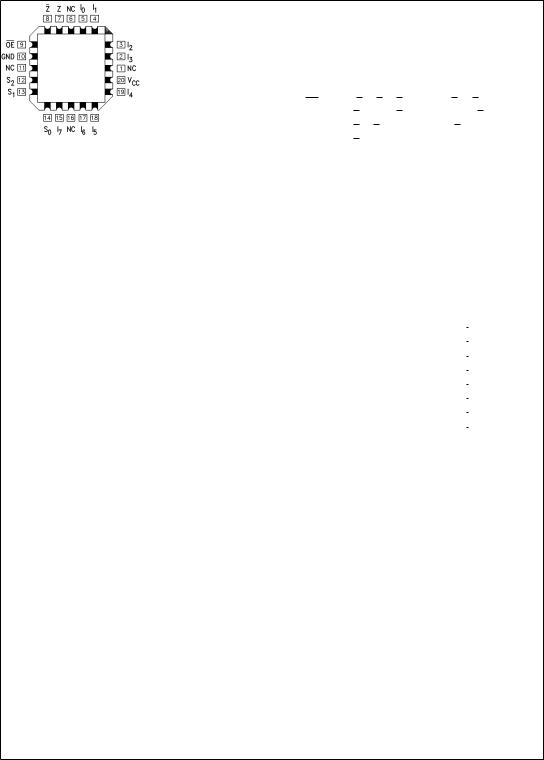
Connection Diagrams
Pin Assignment for DIP and Flatpak
DS100284-3
Pin Assignment
for LCC
DS100284-4
Functional Description
This device is a logical implementation of a single-pole, 8-position switch with the switch position controlled by the state of three Select inputs, S0, S1, S2. Both true and complementary outputs are provided. The Output Enable input ( OE) is active LOW. When it is activated, the logic function provided at the output is:
Z = OE · (I0 · S0 · S1 · S2 + I1· S0 · S1 · S 2 +
I2 · S0 · S 1 · S2 + I3 · S 0 · S1 · S2 +
I4 · S0 · S1 · S2 + I5 · S 0 · S1 · S2 +
I6 · S0 · S 1 · S2 + I7 · S0 · S1 · S2)
When the Output Enable is HIGH, both outputs are in the high impedance (High Z) state. This feature allows multiplexer expansion by tying the outputs of up to 128 devices together. When the outputs of the TRI-STATE devices are tied together, all but one device must be in the high impedance state to avoid high currents that would exceed the maximum ratings. The Output Enable signals should be designed to ensure there is no overlap in the active-LOW portion of the enable voltages.
Truth Table
|
|
|
|
Inputs |
|
|
|
Outputs |
|
|
|
|
|
|
|
|
|
|
|
|
OE |
|
S2 |
S1 |
S0 |
|
Z |
|
Z |
|
H |
X |
X |
X |
|
Z |
Z |
||
|
L |
L |
L |
L |
I0 |
I0 |
|||
|
L |
L |
L |
H |
I1 |
I1 |
|||
|
L |
L |
H |
L |
I2 |
I2 |
|||
|
L |
L |
H |
H |
I3 |
I3 |
|||
|
L |
H |
L |
L |
I4 |
I4 |
|||
|
L |
H |
L |
H |
I5 |
I5 |
|||
|
L |
H |
H |
L |
I6 |
I6 |
|||
|
L |
H |
H |
H |
I7 |
I7 |
|||
H = HIGH Voltage Level
L = LOW Voltage Level
X = Immaterial
Z = High Impedance
www.national.com |
2 |

Logic Diagram
DS100284-5
Please note that this diagram is provided only for the understanding of logic operations and should not be used to estimate propagation delays.
3 |
www.national.com |
 Loading...