


February 1999
54ACT825
8-Bit D Flip-Flop
General Description
The 'ACT825 is an 8-bit buffered register. They have Clock Enable and Clear features which are ideal for parity bus interfacing in high performance microprogramming systems. Also included are multiple enables that allow multi-use control of the interface. The 'ACT825 has noninverting outputs and is fully compatible with AMD's Am29825.
Features
nOutputs source/sink 24 mA
nInputs and outputs are on opposite sides
n'ACT825 has TTL-compatible inputs
nStandard Microcircuit Drawing (SMD)
Ð'ACT825: 5962-91611
Logic Symbols
IEEE/IEC
DS100254-1
DS100254-3
|
|
Pin Names |
Description |
||||||
|
|
|
|
|
|
|
|
|
|
|
D0±D7 |
Data Inputs |
|||||||
|
O0±O7 |
Data Outputs |
|||||||
|
|
|
|
|
2, |
|
3 |
Output Enables |
|
|
OE |
1, |
OE |
OE |
|||||
|
|
|
Clock Enable |
||||||
|
EN |
|
|
||||||
|
|
Clear |
|||||||
|
CLR |
|
|||||||
|
CP |
Clock Input |
|||||||
|
|
|
|
|
|
|
|
|
|
FACT™ is a trademark of Fairchild Semiconductor.
TRI-STATE® is a registered trademark of National Semiconductor Corporation.
Flop-Flip D Bit-8 54ACT825
© 1999 National Semiconductor Corporation |
DS100254 |
www.national.com |
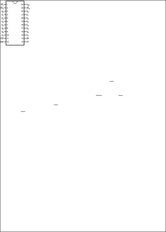
Connection Diagrams
Pin Assignment |
Pin Assignment for LCC |
for DIP and Flatpak |
|
DS100254-2
Functional Description
The 'ACT825 consists of eight D-type edge-triggered flip-flops. These devices have TRI-STATE® outputs for bus systems, organized in a broadside pinning. In addition to the clock and output enable pins, the buffered clock (CP) and buffered Output Enable (OE) are common to all flip-flops. The flip-flops will store the state of their individual D inputs that meet the setup and hold time requirements on the LOW-to-HIGH CP transition. With OE1, OE2 and OE3 LOW, the contents of the flip-flops are available at the outputs. When one of OE1, OE2 or OE3 is HIGH, the outputs go to the high impedance state.
DS100254-4
Operation of the OE input does not affect the state of the flip-flops. The 'ACT825 has Clear (CLR) and Clock Enable (EN) pins. These pins are ideal for parity bus interfacing in high performance systems.
When CLR is LOW and OE is LOW, the outputs are LOW. When CLR is HIGH, data can be entered into the flip-flops. When EN is LOW, data on the inputs is transferred to the outputs on the LOW-to-HIGH clock transition. When EN is HIGH, the outputs do not change state, regardless of the data or clock input transitions.
Function Table
|
|
|
|
|
Inputs |
|
|
Internal |
Output |
Function |
||
|
|
|
|
|
|
|
|
|
|
|
|
|
|
|
|
|
|
|
|
|
CP |
Dn |
Q |
O |
|
OE |
CLR |
EN |
|
|||||||||
|
H |
X |
|
L |
N |
L |
L |
Z |
High-Z |
|||
|
H |
X |
|
L |
N |
H |
H |
Z |
High-Z |
|||
|
H |
L |
|
X |
X |
X |
L |
Z |
Clear |
|||
|
L |
L |
|
X |
X |
X |
L |
L |
Clear |
|||
|
H |
H |
|
H |
X |
X |
NC |
Z |
Hold |
|||
|
L |
H |
|
H |
X |
X |
NC |
NC |
Hold |
|||
|
H |
H |
|
L |
N |
L |
L |
Z |
Load |
|||
|
H |
H |
|
L |
N |
H |
H |
Z |
Load |
|||
|
L |
H |
|
L |
N |
L |
L |
L |
Load |
|||
|
L |
H |
|
L |
N |
H |
H |
H |
Load |
|||
|
|
|
|
|
|
|
|
|
|
|
|
|
H = HIGH Voltage Level
L = LOW Voltage Level
X = Immaterial
Z = High Impedance
N = LOW-to-HIGH Transition
NC = No Change
www.national.com |
2 |

Logic Diagram
DS100254-5
Please note that this diagram is provided only for the understanding of logic operations and should not be used to estimate propagation delays.
3 |
www.national.com |
 Loading...