


NSC 5962-8995001SFA, 5962-8995001SEA, 5962-8995001S2A, 5962-8995001MFA, 5962-8995001M2A Datasheet
...September 1998
54ACT112
Dual JK Negative Edge-Triggered Flip-Flop
General Description
The 'ACT112 contains two independent, high-speed JK flip-flops with Direct Set and Clear inputs. Synchronous state changes are initiated by the falling edge of the clock. Triggering occurs at a voltage level of the clock and is not directly related to the transition time. The J and K inputs can change when the clock is in either state without affecting the flip-flop, provided that they are in the desired state during the recommended setup and hold times relative to the falling edge of the clock. A LOW signal on SD or CD prevents clocking and
forces Q or Q HIGH, respectively. Simultaneous LOW signals on SD and CD force both Q and Q HIGH.
Asynchronous Inputs:
LOW input to SD sets Q to HIGH level
LOW input to CD sets Q to LOW level
Clear and Set are independent of clock
Simultaneous LOW on CD and SD makes both Q and Q HIGH
Features
n'ACT112 has TTL-compatible inputs
nOutputs source/sink 24 mA
nStandard Microcircuit Drawing (SMD) 5962-8995001
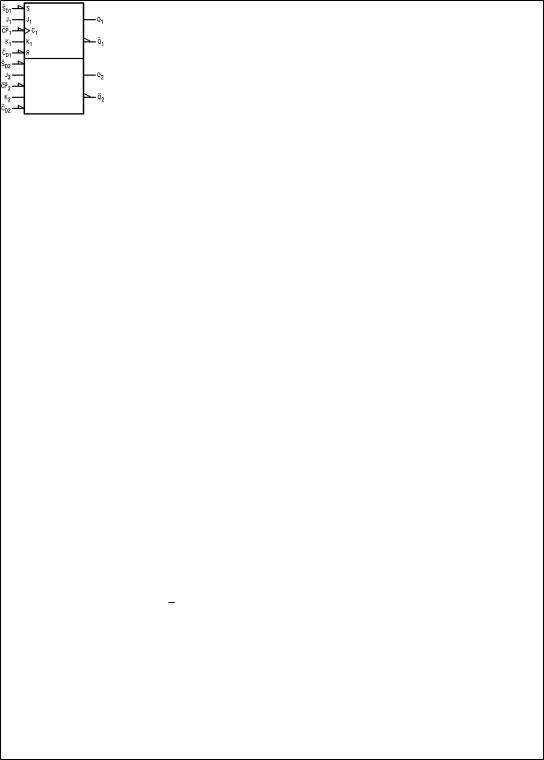
Connection Diagram |
Pin Descriptions |
||||||||||||||||
Pin Assigment for |
|
|
|
|
|
Pin Names |
Description |
||||||||||
|
|
|
|
|
|
|
|
|
|
|
|
|
|
|
|
|
|
|
J1, J2, K1, K2 |
Data Inputs |
|||||||||||||||
DIP and Flatpack |
|
||||||||||||||||
|
|
CP |
1, |
|
|
CP |
2 |
|
|
|
Clock Pulse Inputs |
||||||
|
|
|
|
|
|
|
|
|
|
|
|
|
|
|
|
|
(Active Falling Edge) |
|
|
|
|
|
|
|
D2 |
Direct Clear Inputs (Active LOW) |
|||||||||
|
|
|
C |
D1, |
C |
||||||||||||
|
|
|
|
D2 |
Direct Set Inputs (Active LOW) |
||||||||||||
|
|
S |
D1, |
S |
|||||||||||||
|
|
Q1, Q2, |
Q |
1, |
Q |
2 |
Outputs |
||||||||||
DS100976-3 |
|
|
|
|
|
|
|
|
|
|
|
|
|
|
|
|
|
Pin Assigment
for LCC
DS100976-5
FACT™ is a trademark of Fairchild Semiconductor Corporation.
Flop-Flip Triggered-Edge Negative JK Dual 54ACT112
© 1998 National Semiconductor Corporation |
DS100976 |
www.national.com |
Logic Symbols
DS100976-2
DS100976-1
IEEE/IEC
DS100976-4
Truth Table
|
|
|
|
|
Inputs |
|
|
|
Outputs |
|||||||
|
|
|
|
|
|
|
|
|
|
|
|
|
|
|
|
|
|
|
D |
|
D |
|
|
|
J |
K |
|
Q |
|
|
|
|
|
S |
C |
CP |
Q |
|||||||||||||
|
L |
H |
|
X |
X |
X |
|
H |
|
L |
||||||
|
H |
L |
|
X |
X |
X |
|
L |
|
H |
||||||
|
L |
L |
|
X |
X |
X |
|
H |
|
H |
||||||
|
H |
H |
|
M |
h |
h |
|
|
Q0 |
|||||||
|
|
|
Q |
0 |
||||||||||||
|
H |
H |
|
M |
l |
h |
|
L |
|
H |
||||||
|
H |
H |
|
M |
h |
l |
|
H |
|
L |
||||||
|
H |
H |
|
M |
l |
l |
|
Q0 |
|
|||||||
|
|
|
Q |
0 |
||||||||||||
H (h) = HIGH Voltage Level
L (l) = LOW Voltage Level
X = Immaterial
M = HIGH-to-LOW Clock Transition
Q0 (Q0) = Before HIGH-to-LOW Transition of Clock
Lower case letters indicate the state of the referenced input or output one setup time prior to the HIGH-to-LOW clock transition.
www.national.com |
2 |

Logic Diagram (One Half Shown)
DS100976-6
3 |
www.national.com |
 Loading...