


54F280LMQB
TL/F/9512
54F/74F280 9-Bit Parity Generator/Checker
August 1995
54F/74F280
9-Bit Parity Generator/Checker
General Description
The ’F280 is a high-speed parity generator/checker that ac-
cepts nine bits of input data and detects whether an even or
an odd number of these inputs is HIGH. If an even number
of inputs is HIGH, the Sum Even output is HIGH. If an odd
number is HIGH, the Sum Even output is LOW. The Sum
Odd output is the complement of the Sum Even output.
Features
Y
Guaranteed 4000V minimum ESD protection
Commercial Military
Package
Package Description
Number
74F280PC N14A 14-Lead (0.300
×
Wide) Molded Dual-In-Line
54F280DM (Note 2) J14A 14-Lead Ceramic Dual-In-Line
74F280SC (Note 1) M14A 14-Lead (0.150
×
Wide) Molded Small Outline, JEDEC
74F280SJ (Note 1) M14D 14-Lead (0.300
×
Wide) Molded Small Outline, EIAJ
54F280FM (Note 2) W14B 14-Lead Cerpack
54F280LM (Note 2) E20A 20-Lead Ceramic Leadless Chip Carrier, Type C
Note 1: Devices also available in 13
×
reel. Use suffix
e
SCX and SJX.
Note 2: Military grade device with environmental and burn-in processing. Use suffix
e
DMQB, FMQB and LMQB.
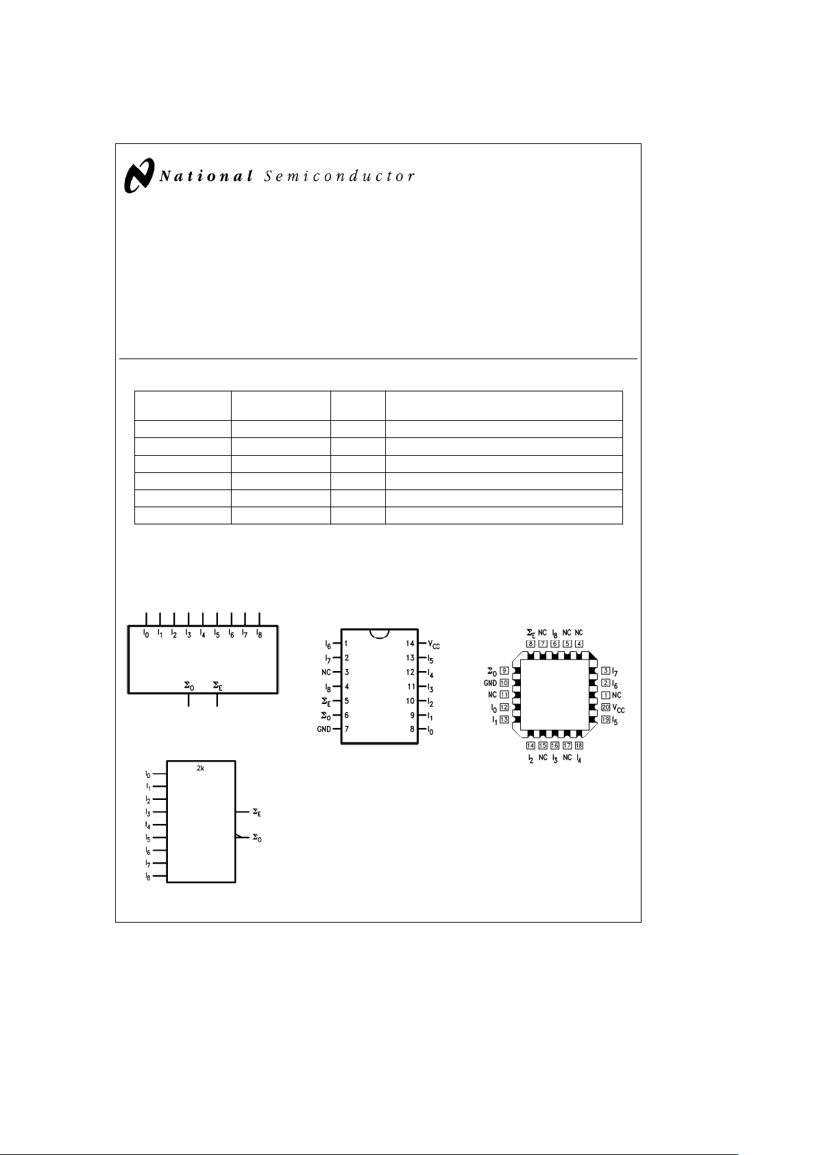
Logic Symbols Connection Diagrams
TL/F/9512– 3
IEEE/IEC
TL/F/9512– 5
Pin Assignment for
DIP, SOIC and Flatpak
TL/F/9512– 1
Pin Assignment
for LCC
TL/F/9512– 2
TRI-STATE
É
is a registered trademark of National Semiconductor Corporation.
C
1995 National Semiconductor Corporation RRD-B30M115/Printed in U. S. A.
Unit Loading/Fan Out
54F/74F
Pin Names Description
U.L. Input I
IH
/I
IL
HIGH/LOW Output I
OH
/I
OL
I
0
–I
8
Data Inputs 1.0/1.0 20 mA/
b
0.6 mA
R
O
Odd Parity Output 50/33.3
b
1 mA/20 mA
R
E
Even Parity Output 50/33.3
b
1 mA/20 mA
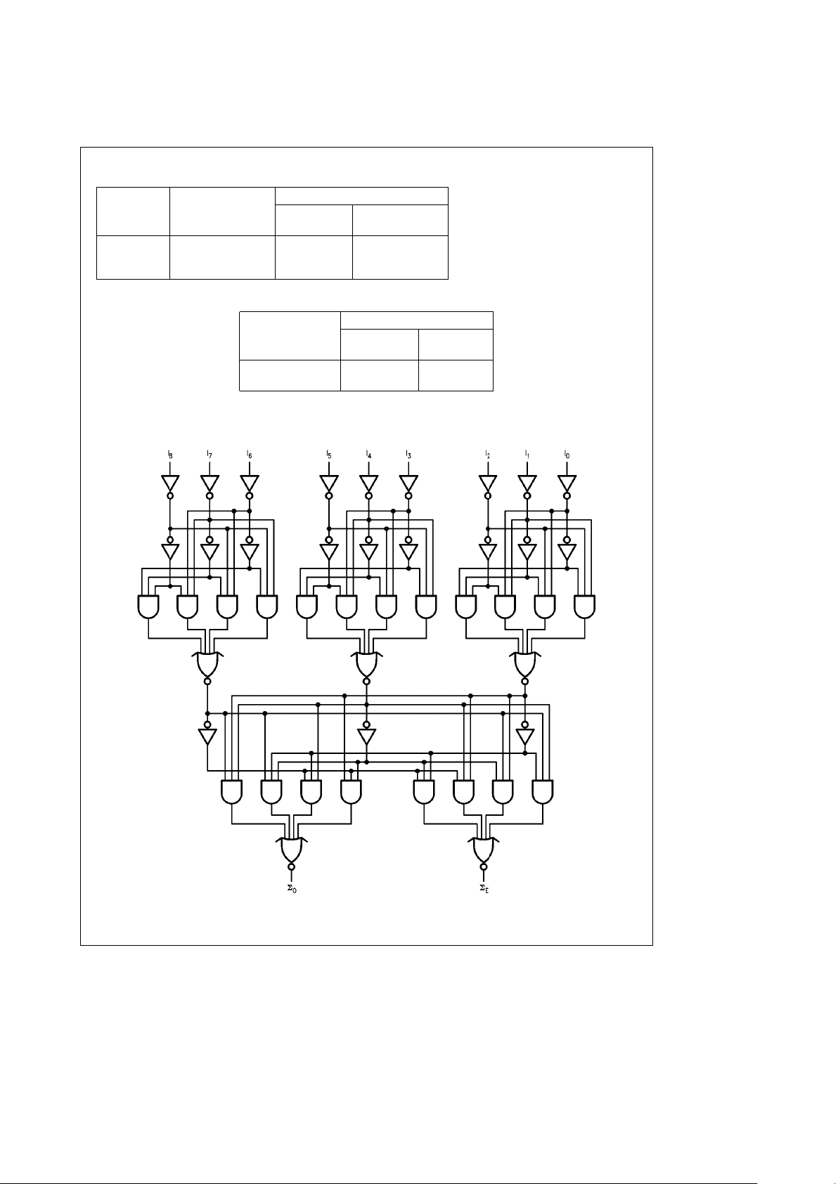
Truth Table
Number of Outputs
HIGH Inputs
R Even R Odd
I
0
–I
8
0, 2, 4, 6, 8 H L
1, 3, 5, 7, 9 L H
H
e
HIGH Voltage Level
L
e
LOW Voltage Level
Logic Diagram
TL/F/9512– 4
Please note that this diagram is provided only for the understanding of logic operations and should not be used to estimate propagation delays.
2
Absolute Maximum Ratings (Note 1)
If Military/Aerospace specified devices are required,
please contact the National Semiconductor Sales
Office/Distributors for availability and specifications.
Storage Temperature
b
65
§
Cto
a
150
§
C
Ambient Temperature under Bias
b
55
§
Cto
a
125
§
C
Junction Temperature under Bias
b
55
§
Cto
a
175
§
C
Plastic
b
55
§
Cto
a
150
§
C
V
CC
Pin Potential to
Ground Pin
b
0.5V to
a
7.0V
Input Voltage (Note 2)
b
0.5V to
a
7.0V
Input Current (Note 2)
b
30 mA to
a
5.0 mA
Voltage Applied to Output
in HIGH State (with V
CC
e
0V)
Standard Output
b
0.5V to V
CC
TRI-STATE
É
Output
b
0.5V to
a
5.5V
Current Applied to Output
in LOW State (Max) twice the rated I
OL
(mA)
ESD Last Passing Voltage (Min) 4000V
Note 1: Absolute maximum ratings are values beyond which the device may
be damaged or have its useful life impaired. Functional operation under
these conditions is not implied.
Note 2: Either voltage limit or current limit is sufficient to protect inputs.
Recommended Operating
Conditions
Free Air Ambient Temperature
Military
b
55
§
Cto
a
125
§
C
Commercial 0
§
Cto
a
70
§
C
Supply Voltage
Military
a
4.5V to
a
5.5V
Commercial
a
4.5V to
a
5.5V
DC Electrical Characteristics
Symbol Parameter
54F/74F
Units V
CC
Conditions
Min Typ Max
V
IH
Input HIGH Voltage 2.0 V Recognized as a HIGH Signal
V
IL
Input LOW Voltage 0.8 V Recognized as a LOW Signal
V
CD
Input Clamp Diode Voltage
b
1.2 V Min I
IN
eb
18 mA
V
OH
Output HIGH 54F 10% V
CC
2.5 I
OH
eb
1mA
Voltage 74F 10% V
CC
2.5 V Min I
OH
eb
1mA
74F 5% V
CC
2.7 I
OH
eb
1mA
V
OL
Output LOW 54F 10% V
CC
0.5
V Min
I
OL
e
20 mA
Voltage 74F 10% V
CC
0.5 I
OL
e
20 mA
I
IH
Input HIGH Current 54F 20.0
mA Max
V
IN
e
2.7V
74F 5.0
I
BVI
Input HIGH Current 54F 100
mA Max
V
IN
e
7.0V
Breakdown Test 74F 7.0
I
CEX
Output HIGH 54F 250
mA Max
V
OUT
e
V
CC
Leakage Current 74F 50
V
ID
Input Leakage Test
74F 4.75 V 0.0
I
ID
e
1.9 mA
All Other Pins Grounded
I
OD
Output Leakage
74F 3.75 mA 0.0
V
IOD
e
150 mV
Circuit Current All Other Pins Grounded
I
IL
Input LOW Current
b
0.6 mA Max V
IN
e
0.5V
I
OS
Output Short-Circuit Current
b
60
b
150 mA Max V
OUT
e
0V
I
CCH
Power Supply Current 25 38 mA Max V
O
e
HIGH
3
 Loading...