


August 1998
100304
Low Power Quint AND/NAND Gate
General Description
The 100304 is monolithic quint AND/NAND gate. The Function output is the wire-NOR of all five AND gate outputs. All inputs have 50 kΩ pull-down resistors.
Features
n Low Power Operation
n2000V ESD protection
nPin/function compatible with 100104
nVoltage compensated operating range = −4.2V to −5.7V
nAvailable to industrial grade temperature range
nAvailable to Standard Microcircuit Drawing (SMD) 5962-9153701
Logic Symbol
DS100304-1
Logic Equation
F = (D1a · D2a) + (D1b · D2b) + D1c · D2c) + (D1d · D2d) + (D1e · D2e).
|
|
Pin Names |
Description |
||
|
|
|
|
|
|
|
Dna±Dne |
Data Inputs |
|||
|
F |
Function Output |
|||
|
Oa±Oe |
Data Outputs |
|||
|
|
|
|
|
|
|
O |
a±O |
e |
Complementary Data Outputs |
|
Gate AND/NAND Quint Power Low 100304
© 1998 National Semiconductor Corporation |
DS100304 |
www.national.com |
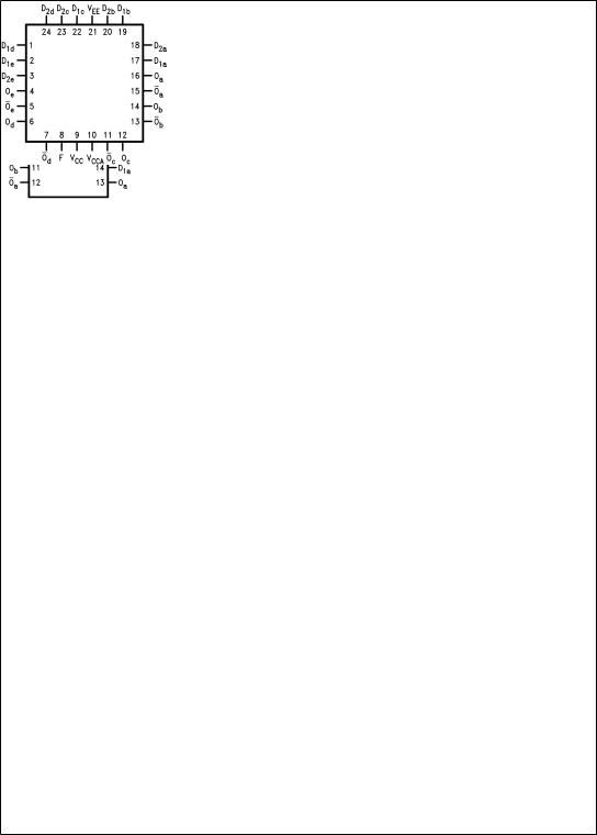
Connection Diagrams
24-Pin DIP |
24-Pin Quad Cerpak |
DS100304-3
DS100304-2
www.national.com |
2 |

Absolute Maximum Ratings (Note 1)
If Military/Aerospace specified devices are required, please contact the National Semiconductor Sales Office/ Distributors for availability and specifications.
Above which the useful life may be impaired
Storage Temperature (TSTG) −65ÊC to +150ÊC Maximum Junction Temperature (TJ)
Ceramic
VEE Pin Potential to Ground Pin Input Voltage (DC)
Output Current (DC Output HIGH)
ESD (Note 2) |
³2000V |
Recommended Operating
Conditions
Case Temperature (TC) |
|
Military |
−55ÊC to +125ÊC |
Supply Voltage (VEE) |
−5.7V to −4.2V |
Note 1: Absolute maximum ratings are those values beyond which the device may be damaged or have its useful life impaired. Functional operation under these conditions is not implied.
Note 2: ESD testing conforms to MIL-STD-883, Method 3015.
Military Version
DC Electrical Characteristics
VEE = −4.2V to −5.7V, V CC = VCCA = GND, TC = −55ÊC to +125ÊC
|
|
|
|
|
|
|
|
|
|
|
Symbol |
Parameter |
Min |
Max |
Units |
TC |
|
Conditions |
Notes |
||
|
VOH |
Output HIGH Voltage |
−1025 |
−870 |
mV |
0ÊC to |
|
|
|
|
|
|
|
|
|
|
+125ÊC |
|
|
|
|
|
|
|
|
|
|
|
|
IN = VIH (Max) |
|
|
|
|
|
−1085 |
−870 |
mV |
−55ÊC |
V |
Loading with |
(Notes 3, 4, 5) |
|
|
VOL |
Output LOW Voltage |
−1830 |
−1620 |
mV |
0ÊC to |
|
or V IL (Min) |
50W0 to −2.0V |
|
|
|
|
|
|
|
+125ÊC |
|
|
|
|
|
|
|
|
|
|
|
|
|
|
|
|
|
|
−1830 |
−1555 |
mV |
−55ÊC |
|
|
|
|
|
|
|
|
|
|
|
|
|
|
|
|
VOHC |
Output HIGH Voltage |
−1035 |
|
mV |
0ÊC to |
|
|
|
|
|
|
|
|
|
|
+125ÊC |
|
|
|
|
|
|
|
|
|
|
|
|
IN = VIH (Min) |
|
|
|
|
|
−1085 |
|
mV |
−55ÊC |
V |
Loading with |
(Notes 3, 4, 5) |
|
|
VOLC |
Output LOW Voltage |
|
−1610 |
mV |
0ÊC to |
|
or V IL (Max) |
50W to −2.0V |
|
|
|
|
|
|
|
+125ÊC |
|
|
|
|
|
|
|
|
|
|
|
|
|
|
|
|
|
|
|
−1555 |
mV |
−55ÊC |
|
|
|
|
|
|
|
|
|
|
|
|
|
|
|
|
VIH |
Input HIGH Voltage |
−1165 |
−870 |
mV |
−55ÊC |
Guaranteed HIGH Signal |
(Notes 3, 4, 5, 6) |
||
|
|
|
|
|
|
+125ÊC |
for All Inputs |
|
|
|
|
|
|
|
|
|
|
|
|
|
|
|
VIL |
Input LOW Voltage |
−1830 |
−1475 |
mV |
−55ÊC to |
Guaranteed LOW Signal |
(Notes 3, 4, 5, 6) |
||
|
|
|
|
|
|
+125ÊC |
for All Inputs |
|
|
|
|
|
|
|
|
|
|
|
|
|
|
|
IIL |
Input LOW Current |
0.50 |
|
µA |
−55ÊC to |
V EE = −4.2V |
|
(Notes 3, 4, 5) |
|
|
|
|
|
|
|
+125ÊC |
VIN = VIL (Min) |
|
|
|
|
|
Input High Current |
|
|
|
|
|
|
|
|
|
|
D2a±D2e |
|
250 |
µA |
0ÊC to |
|
|
|
|
|
|
D1a±D1e |
|
350 |
|
+125ÊC |
VEE = −5.7V |
|
(Notes 3, 4, 5) |
|
|
IIH |
|
|
|
|
|
VIN = VIH (Max) |
|
|
|
|
|
D2a±D2e |
|
350 |
µA |
−55ÊC |
|
|
|
|
|
|
D1a±D1e |
|
500 |
|
|
|
|
|
|
|
IEE |
Power Supply Current |
−75 |
−25 |
mA |
−55ÊC to |
Inputs Open |
|
(Notes 3, 4, 5) |
|
|
|
|
|
|
|
+125ÊC |
|
|
|
|
|
|
|
|
|
|
|
|
|
|
|
Note 3: F100K 300 Series cold temperature testing is performed by temperature soaking (to guarantee junction temperature equals −55ÊC), then testing immed iately without allowing for the junction temperature to stabilize due to heat dissipation after power-up. This provides ªcold startº specs which can be considered a worst case condition at cold temperatures.
Note 4: Screen tested 100% on each device at −55ÊC, +25ÊC, and +125ÊC, Subgroups, 1, 2 3, 7, and 8.
Note 5: Sample tested (Method 5005, Table I) on each manufactured lot at −55ÊC, +25ÊC, and +125ÊC, Subgroups A1, 2, 3, 7, and 8.
Note 6: Guaranteed by applying specified input condition and testing VOH/VOL.
3 |
www.national.com |
 Loading...