


September 1998
54ACTQ16245
16-Bit Transceiver with TRI-STATE® Outputs
General Description
The 'ACTQ16245 contains sixteen non-inverting bidirectional buffers with TRI-STATE outputs and is intended for bus oriented applications. The device is byte controlled. Each has separate control inputs which can be shorted together for full 16-bit operation. The T/R inputs determine the direction of data flow through the device. The OE inputs disable both the A and B ports by placing them in a high impedance state.
The 'ACTQ16245 utilizes NSC Quiet Series technology to guarantee quiet output switching and improved dynamic threshold performance. FACT Quiet Series® features GTO® output control for superior performance.
Features
nUtilizes NSC FACT Quiet Series technology
nGuaranteed simultaneous switching noise level and dynamic threshold performance
nBidirectional non-inverting buffers
nSeparate control logic for each byte
n16-bit version of the 'ACTQ245
nOutputs source/sink 24 mA
nStandard Microcircuit Drawing (SMD) 5962-9562001
Logic Symbol |
Connection Diagram |
|
Pin Assignment for CERPAK |
DS010926-1
Pin Description
|
Pin Names |
Description |
|||
|
|
|
|
|
|
|
|
|
|
Output Enable Input (Active Low) |
|
|
OE |
n |
|||
|
|
|
Transmit/Receive Input |
||
T/R |
|
||||
A0±A15 |
Side A Inputs/Outputs |
||||
B0±B15 |
Side B Outputs/Inputs |
||||
DS010926-2
GTO™ is a trademark of National Semiconductor Corporation.
TRI-STATE® is a registered trademark of National Semiconductor Corporation.
FACT™ and FACT Quiet Series™ are trademarks of Fairchild Semiconductor Corporation.
Outputs STATE-TRI with Transceiver Bit-16 54ACTQ16245
© 1998 National Semiconductor Corporation |
DS010926 |
www.national.com |
Functional Description
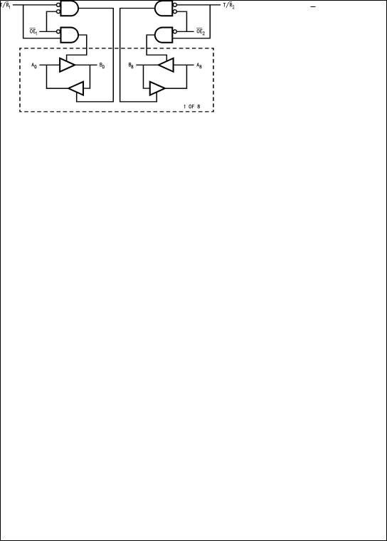
The 'ACTQ16245 contains sixteen non-inverting bidirectional buffers with TRI-STATE outputs. The device is byte controlled with each byte functioning identically, but independent of the other. The control pins can be shorted together to obtain full 16-bit operation. The following description applies to each byte. When the T/R input is HIGH, then Bus A data
is transmitted to Bus B. When the T/R input is LOW, Bus B data is transmitted to Bus A. The TRI-STATE outputs are controlled by an Output Enable (OEn) input for each byte. When OEn is LOW, the outputs are in 2-state mode. When OEn is HIGH, the outputs are in the high impedance mode, but this does not interfere with entering new data into the inputs.
Truth Tables
|
|
|
|
|
Inputs |
Outputs |
|||||
|
|
|
|
1 |
|
|
|
|
|
|
|
OE |
T/R |
1 |
|
|
|||||||
|
|
L |
|
L |
Bus B0±B7 Data to Bus A0±A7 |
||||||
|
|
L |
|
H |
Bus A0±A7 Data to Bus B0±B7 |
||||||
|
|
H |
|
X |
HIGH-Z State on A0±A7, B0±B7 |
||||||
|
|
|
|
|
|
|
|
|
|||
|
|
|
|
Inputs |
|
Outputs |
|||||
|
|
|
|
|
|
|
|
||||
|
|
2 |
|
|
2 |
|
|
||||
OE |
T/R |
|
|
||||||||
|
|
L |
L |
|
Bus B8±B15 Data to Bus A8±A15 |
||||||
|
|
L |
H |
|
Bus A8±A15 Data to Bus B8±B15 |
||||||
|
|
H |
X |
|
HIGH-Z State on A8±A15, B8±B15 |
||||||
H = High Voltage Level
L = Low Voltage Level
X = Immaterial
Z = High Impedance
Logic Diagram
DS010926-3
www.national.com |
2 |
 Loading...