


5962-8976701RA
54FCT540
Octal Buffer/Line Driver with TRI-STATE
®
Outputs
General Description
The ’FCT540 is an octal buffer/line drivers designed to be
employed as memory and address drivers, clock drivers and
bus oriented transmitter/receivers.
These devices are similar in function to the ’FCT240 while
providing flow-through architecture (inputs on opposite side
from outputs).Thispinout arrangement makes these devices
especially useful as output ports for microprocessors, allow-
ing ease of layout and greater PC board density.
Features
n TRI-STATE inverting outputs
n Inputs and outputs opposite side of package, allowing
easier interface to microprocessors
n TTL input and output level compatible
n CMOS power consumption
n Output sink capability of 48mA, source capability of 12
mA
n Standard Microcircuit Drawing (SMD) 5962-8976701
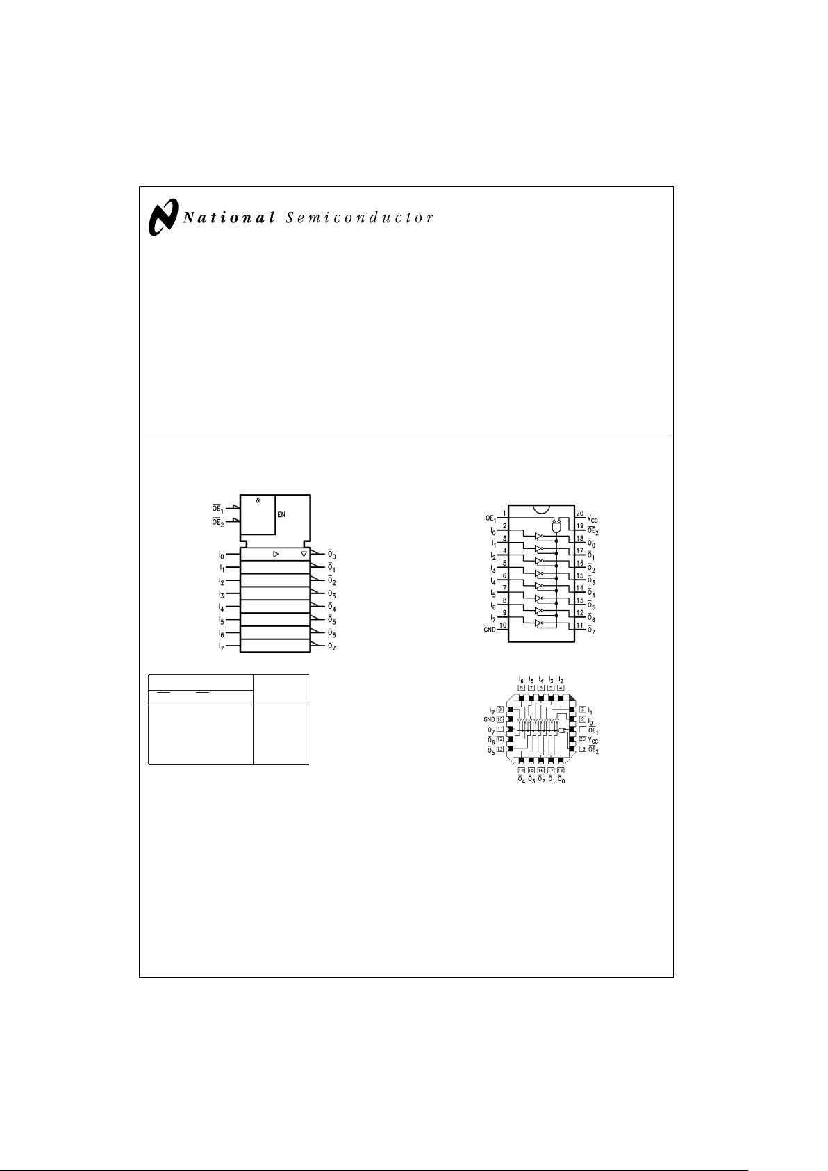
Logic Symbol
Inputs Outputs
OE
1
OE
2
I
LLH L
HXX Z
XHX Z
LLL H
H
=
HIGH Voltage Level
L
=
LOW Voltage Level
X
=
Immaterial
Z
=
High Impedance
Connection Diagrams
TRI-STATE
®
is a registered trademark of National Semiconductor Corporation.
FACT
™
is a trademark of Fairchild Semiconductor Corporation.
IEEE/IEC
DS100970-1
Pin Assignment
for DIP and Flatpak
DS100970-3
Pin Assignment for LCC
DS100970-2
October 1999
54FCT540 Octal Buffer/Line Driver with TRI-STATE Outputs
© 1999 National Semiconductor Corporation DS100970 www.national.com
Absolute Maximum Ratings (Note 1)
If Military/Aerospace specified devices are required,
please contact the National Semiconductor Sales Office/
Distributors for availability and specifications.
Supply Voltage (V
CC
) −0.5V to +7.0V
DC Input Diode Current (I
IK
)
V
I
=
−0.5V −20 mA
V
I
=
V
CC
+ 0.5V +20 mA
DC Input Voltage (V
I
) −0.5V to V
CC
+ 0.5V
DC Output Diode Current (I
OK
)
V
O
=
−0.5V −20 mA
V
O
=
V
CC
+ 0.5V +20 mA
DC Output Voltage (V
O
) −0.5V to V
CC
+ 0.5V
DC Output Source
or Sink Current (I
O
)
±
50 mA
DC V
CC
or Ground Current
per Output Pin (I
CC
or I
GND
)
±
50 mA
Storage Temperature (T
STG
) −65˚C to +150˚C
Junction Temperature (T
J
)
CDIP 175˚C
Recommended Operating
Conditions
Supply Voltage (V
CC
)
’FCT 2.0V to 6.0V
Input Voltage (V
I
) 0VtoV
CC
Output Voltage (V
O
) 0VtoV
CC
Operating Temperature (T
A
)
54FCT −55˚C to +125˚C
Note 1: Absolute maximum ratings are those values beyond which damage
to the device may occur. The databook specifications should be met, without
exception, to ensure that the system design is reliable over its power supply,
temperature, and output/input loading variables. National does not recom-
mend operation of FACT
®
circuits outside databook specifications.
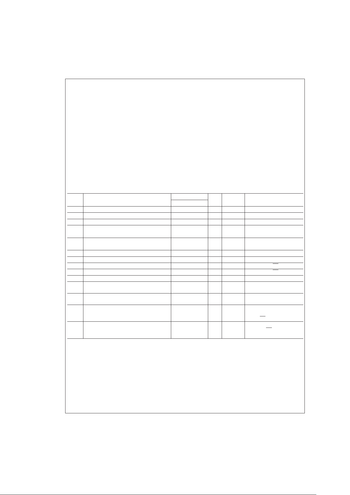
DC Characteristics for ’FCT Family Devices
Symbol Parameter FCT540 Units V
CC
Conditions
Min Max
V
IH
Input HIGH Voltage 2.0 V Recognized HIGH Signal
V
IL
Input LOW Voltage 0.8 V Recognized LOW Signal
V
CD
Input Clamp Diode Voltage −1.2 V Min I
IN
=
−18 mA
V
OH
Output HIGH Voltage 54FCT 4.3 V Min I
OH
=
−300 µA
54FCT 2.4 V Min I
OH
=
−12 mA
V
OL
Output LOW Voltage 54FCT 0.2 V Min I
OL
=
300 µA
54FCT 0.55 V Min I
OL
=
48 mA
I
IH
Input HIGH Current 5 µA Max V
IN
=
V
CC
I
IL
Input LOW Current −5 µA Max V
IN
=
0.0V
I
OZH
Output Leakage Current 10 µA Max V
OUT
=
5.5V; OE
n
=
2.0V
I
OZL
Output Leakage Current −10 µA Max V
OUT
=
0.0V; OE
n
=
2.0V
I
OS
Output Short-Circuit Current -60 mA Max V
OUT
=
0.0V
I
CCQ
Quiescent Power
Supply Current
1.5 mA Max V
IN
<
0.2V or V
IN
5.3V, V
CC
=
5.5V
∆I
CC
Quiescent Power
Supply Current
2.0 mA Max V
I
=
V
CC
− 2.1V
I
CCD
Dynamic I
CC
0.4 mA/
MHz
Max V
CC
= 5.5V, Outputs Open,
One Bit Toggling, 50
%
Duty
Cycle, OE
n
=
GND
I
CC
Total Power Supply
Current
6.0 mA Max V
CC
= 5.5V, Outputs Open, fI
= 10MHz, OE
n
=
GND, One
Bit Toggling, 50
%
Duty Cycle
Note 2: All outputs loaded; thresholds on input associated with output under test.
Note 3: Maximum test duration 2.0 ms, one output loaded at a time.
54FCT540
www.national.com 2
 Loading...