NSC 5962-8765501SA, 5962-8765501RA, 5962-87655012A, 54FCT240MW8, 54FCT240MDA Datasheet

August 1998
54FCT240
Octal Buffer/Line Driver with TRI-STATE® Outputs
General Description
The 54FCT240 is an octal buffer and line driver designed to be employed as a memory address driver, clock driver and bus oriented transmitter or receiver which provides improved PC board density.
Features
nInverting TRI-STATE outputs drive bus lines or buffer memory address registers
nOutput sink capability of 32 mA, source capability of 12 mA
nTTL input and output compatible levels
nCMOS power consumption
nStandard Microcircuit Drawing (SMD) 5962-8765501
Ordering Code:
Military |
Package |
Package Description |
|
Number |
|
|
|
|
54FCT240DMQB |
J20A |
20-Lead Ceramic Dual-In-Line |
|
|
|
54FCT240FMQB |
W20A |
20-Lead Cerpak |
54FCT240LMQB |
E20A |
20-Lead Ceramic Leadless Chip Carrier, Type C |
|
|
|
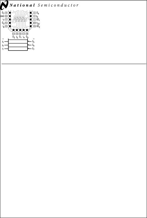
Logic Symbol |
Connection Diagrams |
IEEE/IEC |
Pin Assignment |
|
for DIP and Flatpak |
|
|
|
|
|
|
|
|
|
|
DS100955-2 |
|
|
|
|
|
|
|
|
|
DS100955-1 |
Pin Assignment |
|
|
|
|
|
|
|
|
|
|
for LCC |
|
|
|
|
|
|
|
|
|
|
|
|
|
|
Pin Names |
Description |
|
|||||
|
|
|
|
|
|
|
|
|
|
|
|
|
|
|
|
|
2 |
TRI-STATE Output Enable Inputs |
|
||
|
|
OE |
1, |
OE |
|
|||||
|
I0±I7 |
Inputs |
|
|||||||
|
|
|
|
7 |
Outputs |
|
||||
|
O |
0±O |
|
|||||||
DS100955-3
TRI-STATE® is a registered trademark of National Semiconductor Corporation.
FACT® is a registered trademark of Fairchild Semiconductor Corporation.
Outputs STATE-TRI with Driver Buffer/Line Octal 54FCT240
© 1999 National Semiconductor Corporation |
DS100955 |
www.national.com |

54FCT240
Connection Diagrams (Continued)
|
|
|
|
|
Inputs |
|
Outputs |
||
|
|
|
|
|
|
|
|
|
|
|
OE |
1 |
|
|
In |
|
(Pins 12, 14, 16, 18) |
||
|
|
L |
|
|
L |
|
H |
||
|
|
L |
|
|
H |
|
L |
||
|
|
H |
|
|
X |
|
Z |
||
|
|
|
|
|
|
|
|
|
|
|
|
|
|
|
|
|
|
|
|
|
|
|
|
|
Inputs |
|
Outputs |
||
|
|
|
|
|
|
|
|
|
|
|
|
OE |
2 |
|
|
In |
|
(Pins 3, 5, 7, 9) |
|
|
|
L |
|
|
L |
|
H |
||
|
|
L |
|
|
H |
|
L |
||
|
|
H |
|
|
X |
|
Z |
||
|
|
|
|
|
|
|
|
|
|
H = HIGH Voltage Level
L = LOW Voltage Level
X = Immaterial
Z = High Impedance
www.national.com |
2 |
 Loading...