


5962-9309702MRA
LM1882
•
54ACT715
LM1882-R
•
54ACT715-R Programmable Video Sync
Generator
General Description
The ’ACT715/LM1882 and ’ACT715-R/LM1882-R are 20-pin
TTL-input compatible devices capable of generating Hori-
zontal, Vertical and Composite Sync and Blank signals for
televisions and monitors. All pulse widths are completely de-
finable by the user. The devices are capable of generating
signals for both interlaced and noninterlaced modes of op-
eration. Equalization and serration pulses can be introduced
into the Composite Sync signal when needed.
Four additional signals can also be made available when
Composite Sync or Blank are used. These signals can be
used to generate horizontal or vertical gating pulses, cursor
position or vertical Interrupt signal.
These devices make no assumptions concerning the system
architecture. Line rate and field/frame rate are all a function
of the values programmed into the data registers, the status
register, and the input clock frequency.
The ’ACT715/LM1882 is mask programmed to default to a
Clock Disable state. Bit10oftheStatusRegister,Register 0,
defaults to a logic “0”. This facilitates (re)programming be-
fore operation.
The ’ACT715-R/LM1882-R is the same as the ’ACT715/
LM1882 in all respects except that the ’ACT715-R/
LM1882-R is mask programmed to default to a Clock En-
abled state. Bit 10 of the Status Register defaults to a logic
“1”. Although completely (re)programmable, the ’ACT715-R/
LM1882-R version is better suited for applications using the
default 14.31818 MHz RS-170 register values. This feature
allows power-up directly into operation, following a single
CLEAR pulse.
Features
n Maximum Input Clock Frequency
>
130 MHz
n Interlaced and non-interlaced formats available
n Separate or composite horizontal and vertical Sync and
Blank signals available
n Complete control of pulse width via register
programming
n All inputs are TTL compatible
n 8 mA drive on all outputs
n Default RS170/NTSC values mask programmed into
registers
n 4 KV minimum ESD immunity
n ’ACT715-R/LM1882-R is mask programmed to default to
a Clock Enable state for easier start-up into
14.31818 MHz RS170 timing
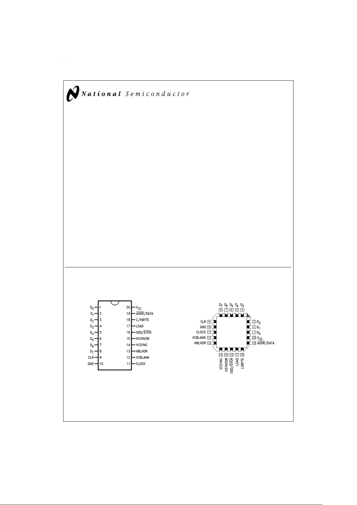
Connection Diagrams
TRI-STATE
®
is a registered trademark of National Semiconductor Corporation.
FACT
™
is a trademark of Fairchild Semiconductor Corporation.
Pin Assignment for
DIP and SOIC
DS100232-1
Order Number LM1882CN or LM1882CM
For Default RS-170, Order Number
LM1882-RCN or LM1882-RCM
Pin Assignment
for LCC
DS100232-2
December 1998
LM1882
•
54ACT715
•
LM1882-R
•
54ACT715-R Programmable Video Sync Generator
© 1998 National Semiconductor Corporation DS100232 www.national.com
Logic Block Diagram
Pin Description
There are a Total of 13 inputs and 5 outputs on the ’ACT715/
LM1882.
Data Inputs D0–D7: The Data Input pins connect to the Ad-
dress Register and the Data Input Register.
ADDR/DATA: The ADDR/DATA signal is latched into the de-
vice on the falling edge of the LOAD signal. The signal deter-
mines if an address (0) or data (1) is present on the data bus.
L/HBYTE: The L/HBYTE signal is latched into the device on
the falling edge of the LOAD signal. The signal determines if
data will be read into the 8 LSB’s (0) or the 4 MSB’s (1) of the
Data Registers. A 1 on this pin when an ADDR/DATA is a 0
enables Auto-Load Mode.
LOAD: The LOAD control pin loads data into the Address or
Data Registers on the rising edge. ADDR/DATA and
L/HBYTE data is loaded into the device on the falling edge of
the LOAD. The LOAD pin has been implemented as a
Schmitt trigger input for better noise immunity.
CLOCK: System CLOCK input from which all timing is de-
rived. The clock pin has been implemented as a Schmitt trig-
ger for better noise immunity. The CLOCK and the LOAD
signal are asynchronous and independent. Output state
changes occur on the falling edge of CLOCK.
CLR: The CLEAR pin is an asynchronous input that initial-
izes the device when it is HIGH. Initialization consists of set-
ting all registers to their mask programmed values, and ini-
tializing all counters, comparators and registers. The CLEAR
pin has been implemented as a Schmitt trigger for better
noise immunity. A CLEAR pulse should be asserted by the
user immediately after power-up to ensure proper initializa-
tion of the registers—even if the user plans to (re)program
the device.
Note: A CLEAR pulse will disable the CLOCK on the ’ACT715/LM1882 and
will enable the CLOCK on the ’ACT715-R/LM1882-R.
ODD/EVEN: Output that identifies if display is in odd (HIGH)
or even (LOW) field of interlace when device is in interlaced
mode of operation. In noninterlaced mode of operation this
output is always HIGH. Data can be serially scanned out on
this pin during Scan Mode.
VCSYNC: Outputs Vertical or Composite Sync signal based
on value of the Status Register. Equalization and Serration
pulses will (if enabled) be output on the VCSYNC signal in
composite mode only.
VCBLANK: Outputs Vertical or Composite Blanking signal
based on value of the Status Register.
HBLHDR: Outputs Horizontal Blanking signal, Horizontal
Gating signal or Cursor Position based on value of the Sta-
tus Register.
HSYNVDR: Outputs Horizontal Sync signal, Vertical Gating
signal or Vertical Interrupt signal based on value of Status
Register.
Register Description
All of the data registers are 12 bits wide. Width’s of all pulses
are defined by specifying the start count and end count of all
pulses. Horizontal pulses are specified with-respect-to the
number of clock pulses per line and vertical pulses are speci-
fied with-respect-to the number of lines per frame.
REG0— STATUS REGISTER
The Status Register controls the mode of operation, the sig-
nals that are output and the polarity of these outputs. The de-
fault value for the Status Register is 0 (000 Hex) for the
’ACT715/LM1882 and is “1024” (400 Hex) for the
’ACT715-R/LM1882-R.
DS100232-3
www.national.com 2
Register Description (Continued)
Bits 0–2
B
2
B
1
B
0
VCBLANK VCSYNC HBLHDR HSYNVDR
0 0 0 CBLANK CSYNC HGATE VGATE
(DEFAULT)
0 0 1 VBLANK CSYNC HBLANK VGATE
0 1 0 CBLANK VSYNC HGATE HSYNC
0 1 1 VBLANK VSYNC HBLANK HSYNC
1 0 0 CBLANK CSYNC CURSOR VINT
1 0 1 VBLANK CSYNC HBLANK VINT
1 1 0 CBLANK VSYNC CURSOR HSYNC
1 1 1 VBLANK VSYNC HBLANK HSYNC
Bits 3–4
B
4
B
3
Mode of Operation
0 0 Interlaced Double Serration and
(DEFAULT) Equalization
0 1 Non Interlaced Double Serration
1 0 Illegal State
1 1 Non Interlaced Single Serration and
Equalization
Double Equalization and Serration mode will output equal-
ization and serration pulses at twice the HSYNC frequency
(i.e., 2 equalization or serration pulses for every HSYNC
pulse). Single Equalization and Serration mode will output
an equalization or serration pulse for every HSYNC pulse. In
Interlaced mode equalization and serration pulses will be
output during the VBLANK period of every odd and even
field. Interlaced Single Equalization and Serration mode is
not possible with this part.
Bits 5–8
Bits 5 through 8 control the polarity of the outputs. A value of
zero in these bit locations indicates an output pulse active
LOW. A value of 1 indicates an active HIGH pulse.
B5— VCBLANK Polarity
B6— VCSYNC Polarity
B7— HBLHDR Polarity
B8— HSYNVDR Polarity
Bits 9–11
Bits 9 through 11 enable several different features of the de-
vice.
B9— Enable Equalization/Serration Pulses (0)
Disable Equalization/Serration Pulses (1)
B10— Disable System Clock (0)
Enable System Clock (1)
Default values for B10 are “0” in the ’ACT715/
LM1882 and “1” in the ’ACT715-R/LM1882-R.
B11— Disable Counter Test Mode (0)
Enable Counter Test Mode (1)
This bit is not intended for the user but is for internal
testing only.
HORIZONTAL INTERVAL REGISTERS
The Horizontal Interval Registers determine the number of
clock cycles per line and the characteristics of the Horizontal
Sync and Blank pulses.
REG1— Horizontal Front Porch
REG2— Horizontal Sync Pulse End Time
REG3— Horizontal Blanking Width
REG4— Horizontal Interval Width
#
of Clocks per
Line
VERTICAL INTERVAL REGISTERS
The Vertical Interval Registers determine the number of lines
per frame, and the characteristics of the Vertical Blank and
Sync Pulses.
REG5— Vertical Front Porch
REG6— Vertical Sync Pulse End Time
REG7— Vertical Blanking Width
REG8— Vertical Interval Width
#
of Lines per Frame
EQUALIZATION AND SERRATION PULSE
SPECIFICATION REGISTERS
These registers determine the width of equalization and ser-
ration pulses and the vertical interval over which they occur.
REG 9 — Equalization Pulse Width End Time
REG10— Serration Pulse Width End Time
REG11— Equalization/Serration Pulse Vertical
Interval Start Time
REG12— Equalization/Serration Pulse Vertical
Interval End Time
VERTICAL INTERRUPT SPECIFICATION REGISTERS
These Registers determine the width of the Vertical Interrupt
signal if used.
REG13— Vertical Interrupt Activate Time
REG14— Vertical Interrupt Deactivate Time
CURSOR LOCATION REGISTERS
These 4 registers determine the cursor position location, or
they generate separate Horizontal and Vertical Gating sig-
nals.
REG15— Horizontal Cursor Position Start Time
REG16— Horizontal Cursor Position End Time
REG17— Vertical Cursor Position Start Time
REG18— Vertical Cursor Position End Time
Signal Specification
HORIZONTAL SYNC AND BLANK
SPECIFICATIONS
All horizontal signals are defined by a start and end time.
The start and end times are specified in number of clock
cycles per line. The start of the horizontal line is considered
pulse 1 not 0. All values of the horizontal timing registers are
referenced to the falling edge of the Horizontal Blank signal
(see
Figure 1
). Since the first CLOCK edge, CLOCK
#
1,
causes the first falling edge of the Horizontal Blank reference
pulse, edges referenced to this first Horizontal edge are n +
1 CLOCKs away, where “n” is the width of the timing in ques-
tion. Registers 1, 2, and 3 are programmed in this manner.
The horizontal counters start at 1 and count until HMAX. The
value of HMAX must be divisible by 2. This limitation is im-
www.national.com3
Signal Specification (Continued)
posed because during interlace operation this value is inter-
nally divided by 2 in order to generate serration and equal-
ization pulses at 2 x the horizontal frequency. Horizontal
signals will change on the falling edge of the CLOCK signal.
Signal specifications are shown below.
Horizontal Period (HPER)
=
REG(4) x ckper
Horizontal Blanking Width:
=
[REG(3) − 1] x ckper
Horizontal Sync Width:
=
[REG(2) − REG(1)] x ckper
Horizontal Front Porch:
=
[REG(1) − 1] x ckper
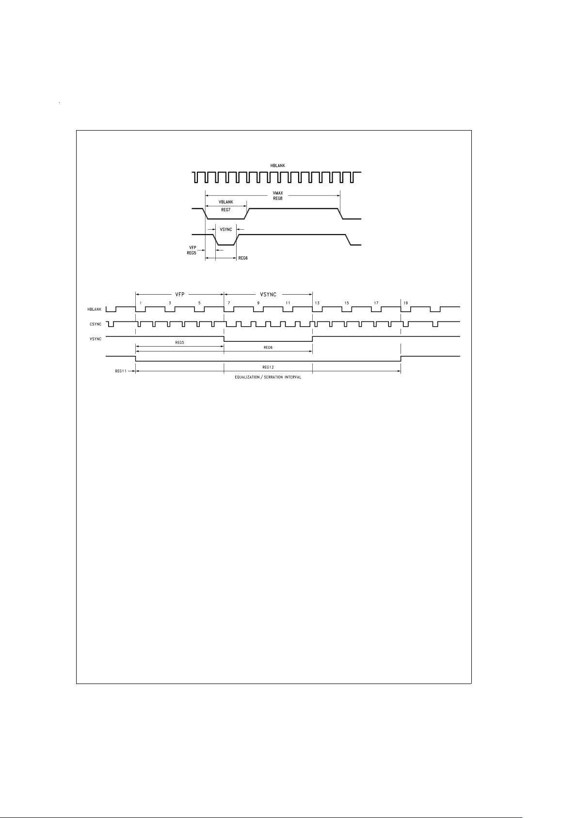
VERTICAL SYNC AND BLANK SPECIFICATION
All vertical signals are defined in terms of number of lines per
frame. This is true in both interlaced and noninterlaced
modes of operation. Care must be taken to not specify the
Vertical Registers in terms of lines per field. Since the first
CLOCK edge, CLOCK
#
1, causes the first falling edge of the
Vertical Blank (first Horizontal Blank) reference pulse, edges
referenced to this first edge aren+1lines away, where “n”
is the width of the timing in question. Registers 5, 6, and 7
are programmed in this manner. Also, in the interlaced
mode, vertical timing is based on half-lines. Therefore regis-
ters 5, 6, and 7 must contain a value twice the total horizontal
(odd and even) plus 1 (as described above). In
non-interlaced mode, all vertical timing is based on
whole-lines. Register 8 is always based on whole-lines and
does not add 1 for the first clock. The vertical counter starts
at the value of 1 and counts until the value of VMAX. No re-
strictions exist on the values placed in the vertical registers.
Vertical Blank will change on the leading edge of HBLANK.
Vertical Sync will change on the leading edge of HSYNC.
(See
Figure 2
.)
Vertical Frame Period (VPER)
=
REG(8) x hper
Vertical Field Period (VPER/n)
=
REG(8) x hper/n
Vertical Blanking Width
=
[REG(7) − 1] x hper/n
Vertical Syncing Width
=
[REG(6) − REG(5)] x hper/n
Vertical Front Porch
=
[REG(5) − 1] x hper/n
where n
=
1 for noninterlaced
n
=
2 for interlaced
COMPOSITE SYNC AND BLANK SPECIFICATION
Composite Sync and Blank signals are created by logically
ANDing (ORing) the active LOW (HIGH) signals of the corre-
sponding vertical and horizontal components of these sig-
nals. The Composite Sync signal may also include serration
and/or equalization pulses. The Serration pulse interval oc-
curs in place of the Vertical Sync interval. Equalization
pulses occur preceding and/or following the Serration
pulses. The width and location of these pulses can be pro-
grammed through the registers shown below.(See
Figure 3
.)
Horizontal Equalization PW
=
[REG(9) − REG(1)] x ckper
REG9
=
(HFP)+(HEQP) + 1
Horizontal Serration PW:
=
[REG(4)/n + REG(1) −
REG(10)] x ckper
REG 10
=
(HFP) +
(HPER/2) − (HSERR) + 1
Where n
=
1 for noninterlaced single serration/
equalization
n
=
2 for noninterlaced double serration/
equalization
n
=
2 for interlaced operation
DS100232-4
FIGURE 1. Horizontal Waveform Specification
www.national.com 4
Signal Specification (Continued)
HORIZONTAL AND VERTICAL GATING SIGNALS
Horizontal Drive and Vertical Drive outputs can be utilized as
general purpose Gating Signals. Horizontal and Vertical Gat-
ing Signals are available for use when Composite Sync and
Blank signals are selected and the value of Bit 2 of the Sta-
tus Register is 0. The Vertical Gating signal will change in the
same manner as that specified for the Vertical Blank.
Horizontal Gating Signal Width
=
[REG(16) − REG(15)] x
ckper
Vertical Gating Signal Width:
=
[REG(18) − REG(17)] x
hper
CURSOR POSITION AND VERTICAL INTERRUPT
The Cursor Position and Vertical Interrupt signal are avail-
able when Composite Sync and Blank signals are selected
and Bit 2 of the Status Register is set to the value of 1. The
Cursor Position generates a single pulse of n clocks wide
during every line that the cursor is specified. The signals are
generated by logically ORing (ANDing) the active LOW
(HIGH) signals specified by the registers used for generating
Horizontal and Vertical Gating signals. The Vertical Interrupt
signal generates a pulse during the vertical interval speci-
fied. The Vertical Interrupt signal will change in the same
manner as that specified for the Vertical Blanking signal.
Horizontal Cursor Width
=
[REG(16) − REG(15)] x ckper
Vertical Cursor Width
=
[REG(18) − REG(17)] x hper
Vertical Interrupt Width
=
[REG(14) − REG(13)] x hper
Addressing Logic
The register addressing logic is composed of two blocks of
logic. The first is the address register and counter (AD-
DRCNTR), and the second is the address decode (AD-
DRDEC).
ADDRCNTR LOGIC
Addresses for the data registers can be generated by one of
two methods. Manual addressing requires that each byte of
each register that needs to be loaded needs to be ad-
dressed. Toload both bytes of all 19 registers would require
a total of 57 load cycles (19 address and 38 data cycles).
Auto Addressing requires that only the initial register value
be specified. The Auto Load sequence would require only 39
load cycles to completely program all registers (1 address
and 38 data cycles). In the auto load sequence the low order
byte of the data register will be written first followed by the
high order byte on the next load cycle. At the time the High
Byte is written the address counter is incremented by 1. The
counter has been implemented to loop on the initial value
loaded into the address register. For example: If a value of 0
was written into the address register then the counter would
count from 0 to 18 before resetting back to 0. If a value of 15
was written into the address register then the counter would
count from 15 to 18 before looping back to 15. If a value
greater than or equal to 18 is placed into the address register
the counter will continuously loop on this value. Auto ad-
dressing is initiated on the falling edge of LOAD when AD-
DRDATA is 0 and LHBYTE is 1. Incrementing and loading of
data registers will not commence until the falling edge of
LOAD after ADDRDATA goes to 1. The next rising edge of
DS100232-5
FIGURE 2. Vertical Waveform Specification
DS100232-12
FIGURE 3. Equalization/Serration Interval Programming
www.national.com5
 Loading...