NSC 5962-9214701VSA, 5962-9214701V2A, 5962-9214701QSA, 5962-9214701QRA, 5962-9214701Q2A Datasheet
...
July 1998
54ABT244
Octal Buffer/Line Driver with TRI-STATE® Outputs
General Description
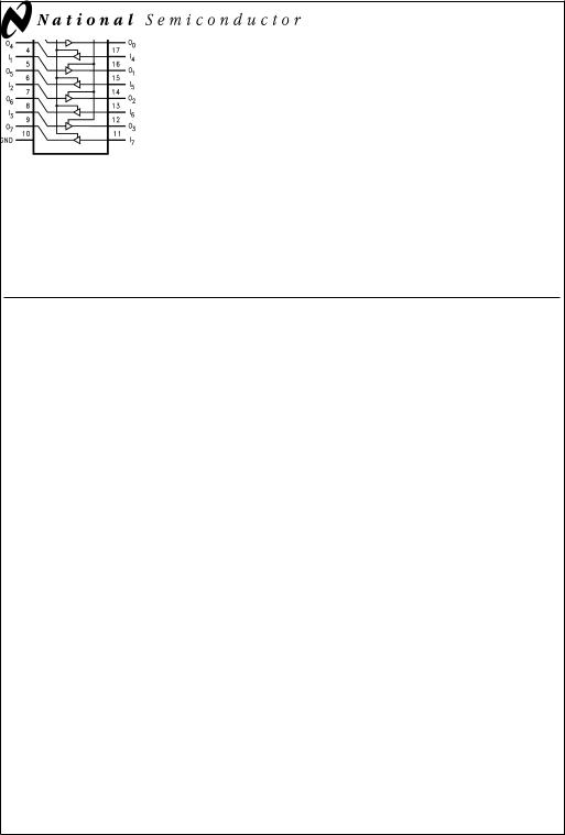
The 'ABT244 is an octal buffer and line driver with TRI-STATE outputs designed to be employed as a memory and address driver, clock driver, or bus-oriented transmitter/ receiver.
Features
nNon-inverting buffers
nOutput sink capability of 48 mA, source capability of 24 mA
nOutput switching specified for both 50 pF and 250 pF loads
nGuaranteed simultaneous switching, noise level and dynamic threshold performance
nGuaranteed latchup protection
nHigh impedance glitch free bus loading during entire power up and power down cycle
nNondestructive hot insertion capability
nDisable time less than enable time to avoid bus contention
nStandard Microcircuit Drawing (SMD) 5962-9214701
Ordering Code
Military |
Package |
Package Description |
|
Number |
|
|
|
|
54ABT244J-QML |
J20A |
20-Lead Ceramic Dual-In-Line |
|
|
|
54ABT244W-QML |
W20A |
20-Lead Cerpack |
|
|
|
54ABT244E-QML |
E20A |
20-Lead Ceramic Leadless Chip Carrier, Type C |
|
|
|
Connection Diagrams
Pin Assignment for |
Pin Assignment for LCC |
DIP and Flatpak |
|
|
|
|
|
|
|
|
|
|
|
|
|
|
|
|
DS100203-2 |
|
|
|
|
|
|
|
DS100203-1 |
|
|
|
|
|
|
|
|
|
|
|
|
|
|
|
|
|
|
Truth Table |
|
|
|
|
|
|
|
||||
|
|
Pin |
Description |
|
|
|
|
|
|
|
|||||||
|
Names |
|
|
|
|
|
|
|
|
|
|
|
|
|
|||
|
|
|
|
OE1 |
I0±3 |
O0±3 |
|
OE2 |
I4±7 |
|
O4±7 |
||||||
|
|
|
|
|
|
|
|
|
|
||||||||
|
|
|
|
|
Output Enable Input |
||||||||||||
|
OE |
1, |
OE |
2 |
|
|
H |
X |
Z |
|
H |
X |
|
Z |
|||
|
|
|
|
|
(Active Low) |
|
|
L |
H |
H |
|
L |
H |
|
H |
||
|
|
|
|
|
|
|
|
|
|
||||||||
|
I0±I7 |
Inputs |
|
|
L |
L |
L |
|
L |
L |
|
L |
|||||
|
O0±O7 |
Outputs |
|
|
|
|
|
|
|
|
|
|
|
|
|||
|
|
H = HIGH Voltage Level |
|
|
|
|
|
|
|||||||||
|
|
|
|
|
|
|
L = LOW Voltage Level |
|
|
|
|
|
|
||||
|
|
|
|
|
|
|
X = Immaterial |
|
|
|
|
|
|
|
|||
|
|
|
|
|
|
|
Z = High Impedance |
|
|
|
|
|
|
||||
TRI-STATE® is a registered trademark of National Semiconductor Corporation.
Outputs STATE-TRI with Driver Buffer/Line Octal 54ABT244
© 1998 National Semiconductor Corporation |
DS100203 |
www.national.com |

Absolute Maximum Ratings (Note 1)
If Military/Aerospace specified devices are required, please contact the National Semiconductor Sales Office/ Distributors for availability and specifications.
Storage Temperature |
−65ÊC to +150ÊC |
Ambient Temperature under Bias |
−55ÊC to +125ÊC |
Junction Temperature under Bias |
|
Ceramic |
−55ÊC to +175ÊC |
VCC Pin Potential to Ground Pin |
−0.5V to +7.0V |
Input Voltage (Note 2) |
−0.5V to +7.0V |
Input Current (Note 2) |
−30 mA to +5.0 mA |
Voltage Applied to Any Output |
|
in the Disabled or |
|
Power-Off State |
−0.5V to 5.5V |
in the HIGH State |
−0.5V to V CC |
Current Applied to Output |
|
in LOW State (Max) |
twice the rated IOL (mA) |
DC Latchup Source Current |
−500 mA |
Over Voltage Latchup (I/O) |
10V |
Recommended Operating
Conditions
Free Air Ambient Temperature |
|
Military |
−55ÊC to +125ÊC |
Supply Voltage |
|
Military |
+4.5V to +5.5V |
Minimum Input Edge Rate |
( V/ t) |
Data Input |
50 mV/ns |
Enable Input |
20 mV/ns |
DC Electrical Characteristics
|
|
|
|
|
|
|
|
|
|
|
|
|
|
Symbol |
Parameter |
|
ABT244 |
Units |
VCC |
|
|
|
Conditions |
||||
|
|
|
|
Min |
Typ Max |
|
|
|
|
|
|
|
|
|
|
|
|
|
|
|
|
|
|
|
|
|
|
|
VIH |
Input HIGH Voltage |
|
2.0 |
|
V |
|
|
Recognized HIGH Signal |
||||
|
VIL |
Input LOW Voltage |
|
|
0.8 |
V |
|
|
Recognized LOW Signal |
||||
|
VCD |
Input Clamp Diode Voltage |
|
−1.2 |
V |
Min |
I IN = −18 mA |
||||||
|
VOH |
Output HIGH Voltage |
54ABT |
2.5 |
|
V |
Min |
|
IOH = −3 mA |
||||
|
|
|
54ABT |
2.0 |
|
V |
Min |
IOH = −24 mA |
|||||
|
VOL |
Output LOW Voltage |
54ABT |
|
0.55 |
V |
Min |
|
IOL = 48 mA |
||||
|
IIH |
Input HIGH Current |
|
|
5 |
µA |
Max |
VIN = 2.7V (Note 4) |
|||||
|
|
|
|
|
5 |
|
|
VIN = VCC |
|||||
|
IBVI |
Input HIGH Current Breakdown Test |
|
7 |
µA |
Max |
VIN = 7.0V |
||||||
|
IIL |
Input LOW Current |
|
|
−5 |
µA |
Max |
V IN = 0.5V (Note 4) |
|||||
|
|
|
|
|
−5 |
|
|
V IN = 0.0V |
|||||
|
VID |
Input Leakage Test |
|
4.75 |
|
V |
0.0 |
|
IID = 1.9 µA |
||||
|
|
|
|
|
|
|
|
All Other Pins Grounded |
|||||
|
|
|
|
|
|
|
|
|
|
|
|
|
|
|
IOZH |
Output Leakage Current |
|
50 |
µA |
0 − 5.5V |
V OUT = 2.7V; |
|
n = 2.0V |
||||
|
|
OE |
|||||||||||
|
IOZL |
Output Leakage Current |
|
−50 |
µA |
0 − 5.5V |
V OUT = 0.5V; |
|
n = 2.0V |
||||
|
|
OE |
|||||||||||
|
IOS |
Output Short-Circuit Current |
−100 |
−275 |
mA |
Max |
V OUT = 0.0V |
||||||
|
ICEX |
Output High Leakage Current |
|
50 |
µA |
Max |
VOUT = VCC |
||||||
|
IZZ |
Bus Drainage Test |
|
|
100 |
µA |
0.0 |
VOUT = 5.5V; All Others GND |
|||||
|
ICCH |
Power Supply Current |
|
|
50 |
µA |
Max |
All Outputs HIGH |
|||||
|
ICCL |
Power Supply Current |
|
|
30 |
mA |
Max |
All Outputs LOW |
|||||
|
ICCZ |
Power Supply Current |
|
|
50 |
µA |
Max |
|
|
n = VCC; |
|||
|
|
|
OE |
||||||||||
|
|
|
|
|
|
|
|
All Others at VCC or Ground |
|||||
|
ICCT |
Additional ICC/Input |
Outputs Enabled |
|
2.5 |
mA |
Max |
|
VI = VCC − 2.1V |
||||
|
|
|
Outputs TRI-STATE |
|
2.5 |
mA |
|
Enable Input VI = VCC − 2.1V |
|||||
|
|
|
Outputs TRI-STATE |
|
50 |
µA |
|
Data Input VI = VCC − 2.1V |
|||||
|
|
|
|
|
|
|
|
All Others at VCC or Ground |
|||||
|
ICCD |
Dynamic ICC |
No Load |
|
|
mA/ |
Max |
|
Outputs Open |
||||
|
|
(Note 4) |
|
|
0.1 |
MHz |
|
|
OE |
n = GND, (Note 3) |
|||
|
|
|
|
|
|
|
|
One Bit Toggling, 50% Duty Cycle |
|||||
|
|
|
|
|
|
|
|
|
|
|
|
|
|
Note 1: Absolute maximum ratings are values beyond which the device may be damaged or have its useful life impaired. Functional operation under these conditions is not implied.
Note 2: Either voltage limit or current limit is sufficient to protect inputs.
Note 3: For 8 bits toggling, ICCD < 0.8 mA/MHz.
Note 4: Guaranteed, but not tested.
www.national.com |
2 |

AC Electrical Characteristics
Symbol |
Parameter |
|
54ABT |
Units |
Fig. |
|
|
|
|
No. |
|
|
|
TA = −55ÊC to +125ÊC |
|
||
|
|
|
VCC = 4.5V±5.5V |
|
|
|
|
|
CL = 50 pF |
|
|
|
|
Min |
Max |
|
|
|
|
|
|
|
|
tPLH |
Propagation Delay |
1.0 |
5.3 |
ns |
Figure 5 |
tPHL |
Data to Outputs |
1.0 |
5.0 |
|
|
tPZH |
Output Enable |
0.8 |
6.5 |
ns |
Figure 4 |
tPZL |
Time |
1.2 |
7.9 |
|
|
tPHZ |
Output Disable |
1.2 |
7.6 |
ns |
Figure 4 |
tPLZ |
Time |
1.0 |
7.9 |
|
|
Capacitance
Symbol |
|
Parameter |
|
Typ |
|
Units |
|
Conditions |
|
|
|
|
|
|
|
|
TA = 25ÊC |
CIN |
|
Input Capacitance |
|
5.0 |
|
pF |
|
VCC = 0V |
COUT (Note 5) |
|
Output Capacitance |
|
9.0 |
|
pF |
|
VCC = 5.0V |
Note 5: COUT is measured at frequency f = 1 MHz, per MIL-STD-883B, Method 3012. |
|
|
|
|
|
|||
|
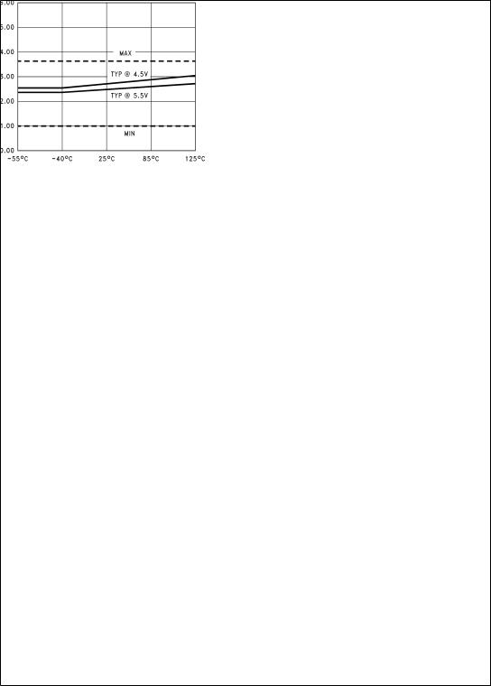
tPLH vs Temperature (TA) |
|
tPHL vs Temperature (TA) |
|
||||
CL = 50 pF, 1 Output Switching |
|
CL = 50 pF, 1 Output Switching |
||||||
DS100203-11 |
DS100203-12 |
Dashed lines represent design characteristics; for specified guarantees refer to AC Characteristics Table.
3 |
www.national.com |
 Loading...