


5962-8755301EA
54AC139•54ACT139
Dual 1-of-4 Decoder/Demultiplexer
General Description
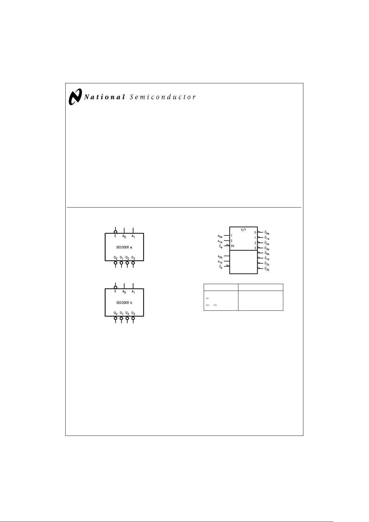
The ’AC/’ACT139 is a high-speed, dual 1-of-4 decoder/
demultiplexer. The device has two independent decoders,
each accepting two inputs and providing four
mutually-exclusive active-LOW outputs. Each decoder has
an active-LOW Enable input which can be used as a data input for a 4-output demultiplexer. Each half of the ’AC/
’ACT139 can be used as a function generator providing all
four minterms of two variables.
Features
n ICCreduced by 50
%
n Multifunction capability
n Two completely independent 1-of-4 decoders
n Active LOW mutually exclusive outputs
n Outputs source/sink 24 mA
n ’ACT139 has TTL-compatible inputs
n Standard Military Drawing (SMD)
—’AC139: 5962-87623
—’ACT139: 5962-87553
Logic Symbols
Pin Names Description
A
0,A1
Address Inputs
E
Enable Inputs
O
0–O3
Outputs
FACT®is a registeredtrademark of Fairchild Semiconductor Corporation.
DS100269-8
DS100269-1
IEEE/IEC
DS100269-2
August 1998
54AC139
•
54ACT139 Dual 1-of-4 Decoder/Demultiplexer
© 1998 National Semiconductor Corporation DS100269 www.national.com
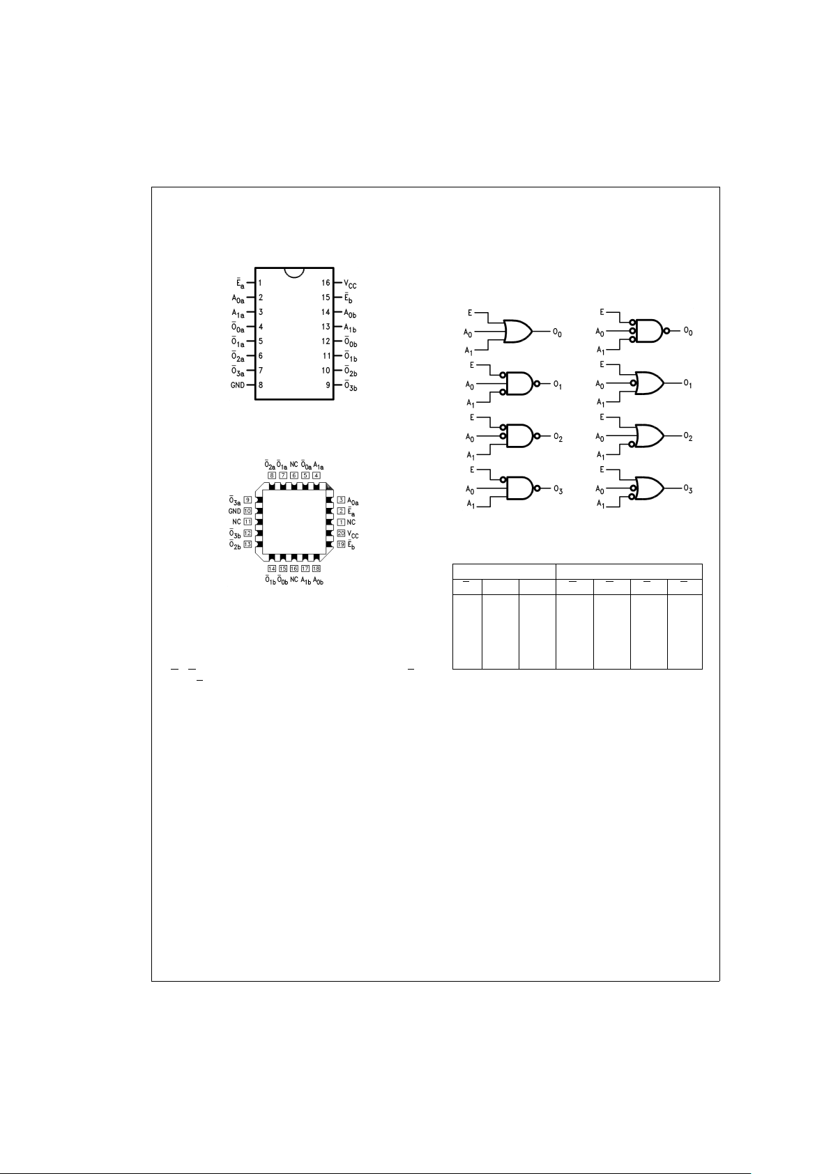
Connection Diagrams
Functional Description
The ’AC/’ACT139 is a high-speed dual 1-of-4 decoder/
demultiplexer. The device has two independent decoders,
each of which accepts two binary weighted inputs (A
0–A1
)
and provides four mutually exclusive active-LOW outputs
(O
0–O3
). Each decoder has an active-LOW enable (E).
When E is HIGH all outputs are forced HIGH. The enable
can be used as the data input for a 4-output demultiplexer
application. Each half of the ’AC/’ACT139 generates all four
minterms of two variables. These four minterms are useful in
some applications, replacing multiple gate functions as
shown in , and thereby reducing the number of packages required in a logic network.
Truth Table
Inputs Outputs
E
A
0
A
1
O
0
O
1
O
2
O
3
HXXHHHH
LLLLHHH
LHLHLHH
LLHHHLH
LHHHHHL
H
=
HIGH Voltage Level
L=LOW Voltage Level
X=Immaterial
Pin Assignment
for DIP and Flatpak
DS100269-3
Pin Assignment
for LCC
DS100269-4
DS100269-6
FIGURE 1. Gate Functions (Each Half)
www.national.com 2
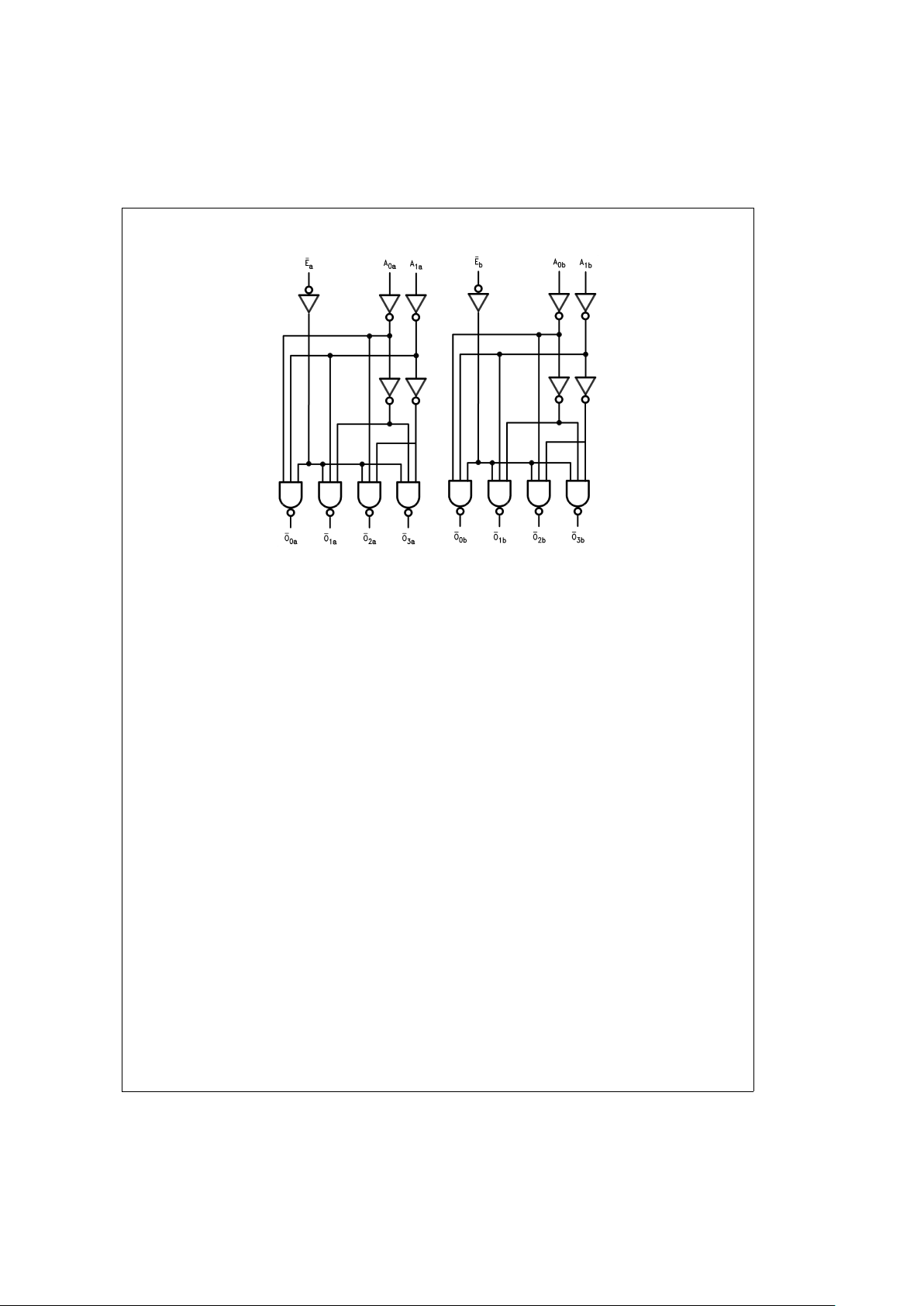
Logic Diagram
DS100269-5
Please note that this diagram is provided only for the understanding of logic operations and should not be used to estimate propagation delays.
3 www.national.com
 Loading...