


NSC 5962R8766301SSA, 5962R8766301SRA, 5962R8766301S2A, 5962R8766301BSA, 5962R8766301BRA Datasheet
...
August 1998
54AC245 · 54ACT245
Octal Bidirectional Transceiver with TRI-STATE®
Inputs/Outputs
General Description
The 'AC/'ACT245 contains eight non-inverting bidirectional buffers with TRI-STATE outputs and is intended for bus-oriented applications. Current sinking capability is 24 mA at both the A and B ports. The Transmit/Receive (T/R) input determines the direction of data flow through the bidirectional transceiver. Transmit (active-HIGH) enables data from A ports to B ports; Receive (active-LOW) enables data from B ports to A ports. The Output Enable input, when HIGH, disables both A and B ports by placing them in a HIGH Z condition.
Features
nICC and IOZ reduced by 50%
nNoninverting buffers
nBidirectional data path
nA and B outputs source/sink 24 mA
n'ACT245 has TTL-compatible inputs
nStandard Microcircuit Drawing (SMD)
Ð'AC245: 5962-87758
Ð'ACT245: 5962-87663
Logic Symbols
IEEE/IEC
DS100283-1
DS100283-2
|
|
|
|
Pin |
Description |
|
|
Names |
|
||
|
|
|
|
|
|
|
|
|
Output Enable Input |
||
|
OE |
|
|
||
|
|
|
Transmit/Receive Input |
||
T/R |
|
||||
A0±A7 |
Side A TRI-STATE Inputs or TRI-STATE Outputs |
||||
B0±B7 |
Side B TRI-STATE Inputs or TRI-STATE Outputs |
||||
TRI-STATE® is a registered trademark of National Semiconductor Corporation.
FACT® is a registered trademark of Fairchild Semiconductor Corporation.
Inputs/Outputs STATE-TRI with Transceiver Bidirectional Octal 54ACT245 · 54AC245
© 1998 National Semiconductor Corporation |
DS100283 |
www.national.com |
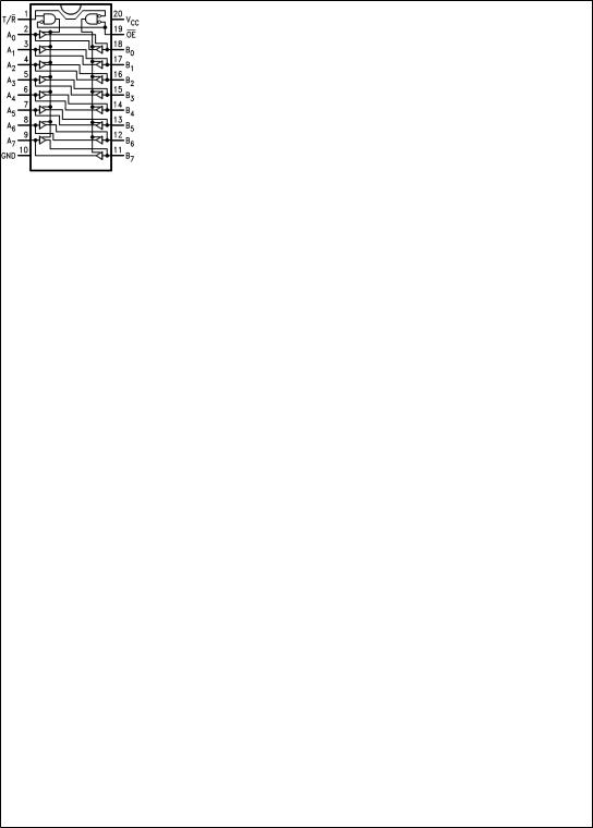
Connection Diagrams
Pin Assignment for |
Pin Assignment for LCC |
DIP and Flatpak |
|
|
|
|
|
|
|
|
|
DS100283-4 |
|
Truth Table |
|
|
|
|
|||
|
|
|
|
|
|
|
|
|
|
|
|
Inputs |
|
|
|
Outputs |
|
|
|
|
|
|
|
|
|
|
|
|
OE |
|
|
T/R |
|
|
|
DS100283-3 |
|
|
|
|
|
|
|
|
|
L |
|
L |
Bus B Data to Bus A |
||||
|
|
|
||||||
|
|
L |
|
H |
Bus A Data to Bus B |
|||
|
|
H |
|
X |
HIGH-Z State |
|||
|
|
|
|
|
|
|
|
|
H = HIGH Voltage Level
L = LOW Voltage Level
X = Immaterial
www.national.com |
2 |

Absolute Maximum Ratings (Note 1)
If Military/Aerospace specified devices are required, please contact the National Semiconductor Sales Office/ Distributors for availability and specifications.
Supply Voltage (VCC) |
−0.5V to +7.0V |
DC Input Diode Current (IIK) |
|
VI = −0.5V |
−20 mA |
VI = VCC + 0.5V |
+20 mA |
DC Input Voltage (VI) |
−0.5V to V CC + 0.5V |
DC Output Diode Current (IOK) |
|
VO = −0.5V |
−20 mA |
VO = VCC + 0.5V |
+20 mA |
DC Output Voltage (VO) |
−0.5V to V CC + 0.5V |
DC Output Source |
|
or Sink Current (IO) |
±50 mA |
DC VCC or Ground Current |
|
per Output Pin (ICC or IGND) |
±50 mA |
Storage Temperature (TSTG) |
−65ÊC to +150ÊC |
Junction Temperature (TJ) |
|
CDIP |
175ÊC |
Recommended Operating
Conditions
Supply Voltage (VCC) |
|
|
'AC |
|
2.0V to 6.0V |
'ACT |
|
4.5V to 5.5V |
Input Voltage (VI) |
|
0V to VCC |
Output Voltage (VO) |
|
0V to VCC |
Operating Temperature (TA) |
|
|
54AC/ACT |
|
−55ÊC to +125ÊC |
Minimum Input Edge Rate ( |
V/ |
t) |
'AC Devices |
|
|
VIN from 30% to 70% of VCC |
|
|
VCC @ 3.3V, 4.5V, 5.5V |
|
125 mV/ns |
Minimum Input Edge Rate ( |
V/ |
t) |
'ACT Devices |
|
|
VIN from 0.8V to 2.0V |
|
|
VCC @ 4.5V, 5.5V |
|
125 mV/ns |
Note 1: Absolute maximum ratings are those values beyond which damage to the device may occur. The databook specifications should be met, without exception, to ensure that the system design is reliable over its power supply, temperature, and output/input loading variables. National does not recommend operation of FACT® circuits outside databook specifications.
DC Characteristics for 'AC Family Devices
|
|
|
54AC |
|
|
|
|
|
|
|
|
|
|
Symbol |
Parameter |
VCC |
TA = |
Units |
Conditions |
|
|
|
(V) |
−55ÊC to +125ÊC |
|
|
|
|
|
|
|
|
|
|
|
|
|
Guaranteed |
|
|
|
|
|
|
Limits |
|
|
|
VIH |
Minimum High |
3.0 |
2.1 |
|
VOUT = 0.1V |
|
|
Level Input |
4.5 |
3.15 |
V |
or VCC − 0.1V |
|
|
Voltage |
5.5 |
3.85 |
|
|
|
|
|
|
|
|
|
|
VIL |
Maximum Low |
3.0 |
0.9 |
|
VOUT = 0.1V |
|
|
Level Input |
4.5 |
1.35 |
V |
or VCC − 0.1V |
|
|
Voltage |
5.5 |
1.65 |
|
|
|
|
|
|
|
|
|
|
VOH |
Minimum High |
3.0 |
2.9 |
|
IOUT = −50 µA |
|
|
Level Output |
4.5 |
4.4 |
V |
|
|
|
Voltage |
5.5 |
5.4 |
|
|
|
|
|
|
|
|
|
|
|
|
|
|
|
(Note 2) |
|
|
|
|
|
|
VIN = VIL or VIH |
|
|
|
3.0 |
2.4 |
|
|
−12 mA |
|
|
4.5 |
3.7 |
V |
IOH |
−24 mA |
|
|
5.5 |
4.7 |
|
|
−24 mA |
|
|
|
|
|
|
|
VOL |
Maximum Low |
3.0 |
0.1 |
|
IOUT = 50 µA |
|
|
Level Output |
4.5 |
0.1 |
V |
|
|
|
Voltage |
5.5 |
0.1 |
|
|
|
|
|
|
|
|
|
|
|
|
|
|
|
(Note 2) |
|
|
|
|
|
|
VIN = VIL or VIH |
|
|
|
3.0 |
0.50 |
|
|
12 mA |
|
|
4.5 |
0.50 |
V |
IOL |
24 mA |
|
|
5.5 |
0.50 |
|
|
24 mA |
|
|
|
|
|
|
|
IIN |
Maximum Input |
5.5 |
±1.0 |
µA |
VI = VCC, GND |
|
|
Leakage Current |
|
|
|
|
|
|
|
|
|
|
|
|
3 |
www.national.com |
 Loading...