


NSC 5962-8968201LA, 5962-89682013A, 5962-8968201KA, 54AC646SDMQB-RH, 54AC646MDA Datasheet
...
August 1998
54AC646
Octal Transceiver/Register with TRI-STATE® Outputs
General Description
The 'AC646 consist of registered bus transceiver circuits, with outputs, D-type flip-flops and control circuitry providing multiplexed transmission of data directly from the input bus or from the internal storage registers. Data on the A or B bus will be loaded into the respective registers on the LOW-to-HIGH transition of the appropriate clock pin (CPAB or CPBA). The four fundamental data handling functions available are illustrated in Figures 1, 2, 3, 4.
nMultiplexed real-time and stored data transfers
nTRI-STATE outputs
n300 mil slim dual-in-line package
nOutputs source/sink 24 mA
n'ACT646 has TTL compatible inputs
nStandard Microcircuit Drawing (SMD)
Ð'AC646: 5962-89682
Features
n Independent registers for A and B buses
Logic Symbols
DS100231-1
|
|
Pin Names |
Description |
|
|
|
|
|
A0±A7 |
Data Register A Inputs |
|
|
|
|
Data Register A Outputs |
|
B0±B7 |
Data Register B Inputs |
|
|
|
|
Data Register B Outputs |
|
CPAB, CPBA |
Clock Pulse Inputs |
|
|
SAB, SBA |
Transmit/Receive Inputs |
|
|
|
Output Enable Input |
|
|
G |
|
|
|
DIR |
Direction Control Input |
|
IEEE/IEC
DS100231-2
TRI-STATE® is a registered trademark of National Semiconductor Corporation. FACT® is a registered trademark of Fairchild Semiconductor Corporation.
Outputs STATE-TRI with Transceiver/Register Octal 54AC646
© 1998 National Semiconductor Corporation |
DS100231 |
www.national.com |
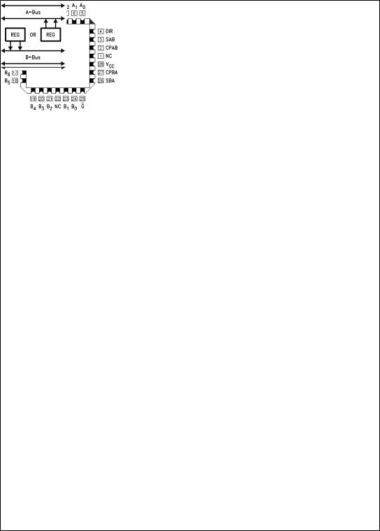
Connection Diagrams
Pin Assignment for DIP and Flatpak
DS100231-3
Real Time Transfer
A-Bus to B-Bus
DS100231-7
FIGURE 1.
Real Time Transfer
B-Bus to A-Bus
DS100231-8
FIGURE 2.
Pin Assignment
for LCC
DS100231-4
Storage from
Bus to Register
DS100231-9
FIGURE 3.
Transfer from
Register to Bus
DS100231-10
FIGURE 4.
www.national.com |
2 |

Function Table
|
|
|
Inputs |
|
|
Data I/O (Note 1) |
Function |
|
|
|
|
|
|
|
|
|
|
G |
DIR |
CPAB |
CPBA |
SAB |
SBA |
A0±A7 |
B0±B7 |
|
H |
X |
H or L |
H or L |
X |
X |
|
|
Isolation |
H |
X |
N |
X |
X |
X |
Input |
Input |
Clock An Data into A Register |
|
||||||||
H |
X |
X |
N |
X |
X |
|
|
Clock Bn Data into B Register |
|
|
|
||||||
L |
H |
X |
X |
L |
X |
|
|
An to Bn Ð Real Time (Transparent Mode) |
L |
H |
N |
X |
L |
X |
Input |
Output |
Clock An Data into A Register |
|
||||||||
L |
H |
H or L |
X |
H |
X |
|
|
A Register to Bn (Stored Mode) |
L |
H |
N |
X |
H |
X |
|
|
Clock An Data into A Register and Output to Bn |
|
|
|
||||||
L |
L |
X |
X |
X |
L |
|
|
Bn to An Ð Real Time (Transparent Mode) |
L |
L |
X |
N |
X |
L |
Output |
Input |
Clock Bn Data into B Register |
|
||||||||
L |
L |
X |
H or L |
X |
H |
|
|
B Register to An (Stored Mode) |
L |
L |
X |
N |
X |
H |
|
|
Clock Bn Data into B Register and Output to An |
|
|
|
||||||
H = HIGH Voltage Level
L = LOW Voltage Level
X = Immaterial
N = LOW-to-HIGH Transition
Note 1: The data output functions may be enabled or disabled by various signals at the G and DIR inputs. Data input functions are always enabled; i.e., data at the bus pins will be stored on every LOW-to-HIGH transition of the appropriate clock inputs.
3 |
www.national.com |
 Loading...