


NSC ADC0834MWC, ADC0834MDC, ADC0834CIWMX, ADC0834CIWM, ADC0834CCJ Datasheet
...July 2002
ADC0831/ADC0832/ADC0834/ADC0838
8-Bit Serial I/O A/D Converters with Multiplexer Options
General Description
The ADC0831 series are 8-bit successive approximation A/D converters with a serial I/O and configurable input multiplexers with up to 8 channels. The serial I/O is configured to comply with the NSC MICROWIRE™ serial data exchange standard for easy interface to the COPS™ family of processors, and can interface with standard shift registers or µPs.
The 2-, 4- or 8-channel multiplexers are software configured for single-ended or differential inputs as well as channel assignment.
The differential analog voltage input allows increasing the common-mode rejection and offsetting the analog zero input voltage value. In addition, the voltage reference input can be adjusted to allow encoding any smaller analog voltage span to the full 8 bits of resolution.
Features
nNSC MICROWIRE compatible — direct interface to COPS family processors
nEasy interface to all microprocessors, or operates “stand-alone”
nOperates ratiometrically or with 5 VDC voltage reference
nNo zero or full-scale adjust required
n2-, 4- or 8-channel multiplexer options with address logic
nShunt regulator allows operation with high voltage supplies
n0V to 5V input range with single 5V power supply
nRemote operation with serial digital data link
nTTL/MOS input/output compatible
n0.3" standard width, 8-, 14or 20-pin DIP package
n20 Pin Molded Chip Carrier Package (ADC0838 only)
nSurface-Mount Package
Key Specifications
n Resolution |
8 Bits |
|
n Total Unadjusted Error |
±1⁄2 LSB and ±1 LSB |
|
n Single Supply |
5 VDC |
|
n |
Low Power |
15 mW |
n |
Conversion Time |
32 µs |
Typical Application
00558301
TRI-STATE® is a registered trademark of National Semiconductor Corporation.
COPS™ and MICROWIRE™ are trademarks of National Semiconductor Corporation.
Options Multiplexer with Converters A/D I/O Serial Bit-8 ADC0831/ADC0832/ADC0834/ADC0838
© 2002 National Semiconductor Corporation |
DS005583 |
www.national.com |
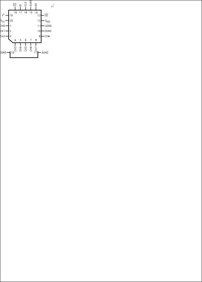
ADC0831/ADC0832/ADC0834/ADC0838
Connection Diagrams
ADC0838 8-Channel Mux
Small Outline/Dual-In-Line Package (WM and N)
00558308
Top View
ADC0834 4-Channel MUX
Small Outline/Dual-In-Line Package (WM and N)
00558330
COM internally connected to A GND
Top View
Top View
ADC0832 2-Channel MUX
Dual-In-Line Package (N)
00558331
COM internally connected to GND.
VREF internally connected to VCC.
Top View
Top View
ADC0832 2-Channel MUX
Small Outline Package (WM)
00558341
Top View
ADC0831 Single
Differential Input
Dual-In-Line Package (N)
00558332
Top View
ADC0831 Single Differential Input
Small Outline Package (WM)
00558342
Top View
ADC0838 8-Channel MUX
Molded Chip Carrier (PCC) Package (V)
00558333
www.national.com |
2 |

Ordering Information
Part Number |
Analog Input |
Total |
Package |
Temperature |
|
Channels |
Unadjusted Error |
|
Range |
|
|
|
|
|
ADC0831CCN |
1 |
±1 |
Molded (N) |
0˚C to +70˚C |
ADC0831CCWM |
|
|
SO(M) |
0˚C to +70˚C |
|
|
|
|
|
ADC0832CIWM |
2 |
±1 |
SO(M) |
−40˚C to +85˚C |
ADC0832CCN |
|
|
Molded (N) |
0˚C to +70˚C |
ADC0832CCWM |
|
|
SO(M) |
0˚C to +70˚C |
|
|
|
|
|
ADC0834BCN |
4 |
±1⁄2 |
Molded (N) |
0˚C to +70˚C |
ADC0834CCN |
|
±1 |
Molded (N) |
0˚C to +70˚C |
ADC0834CCWM |
|
|
SO(M) |
0˚C to +70˚C |
|
|
|
|
|
ADC0838BCV |
8 |
±1⁄2 |
PCC (V) |
0˚C to +70˚C |
ADC0838CCV |
|
±1 |
PCC (V) |
0˚C to +70˚C |
ADC0838CCN |
|
|
Molded (N) |
0˚C to +70˚C |
ADC0838CIWM |
|
|
SO(M) |
−40˚C to +85˚C |
ADC0838CCWM |
|
|
SO(M) |
0˚C to +70˚C |
|
|
|
|
|
See NS Package Number M14B, M20B, N08E, N14A,
N20A or V20A
ADC0831/ADC0832/ADC0834/ADC0838
3 |
www.national.com |

ADC0831/ADC0832/ADC0834/ADC0838
Absolute Maximum Ratings (Notes 1,
2)
If Military/Aerospace specified devices are required, please contact the National Semiconductor Sales Office/ Distributors for availability and specifications.
Current into V+ (Note 3) |
15 mA |
Supply Voltage, VCC (Note 3) |
6.5V |
Voltage |
|
Logic Inputs |
−0.3V to VCC + |
|
0.3V |
Analog Inputs |
−0.3V to VCC + |
|
0.3V |
Input Current per Pin (Note 4) |
±5 mA |
Package |
±20 mA |
Storage Temperature |
−65˚C to +150˚C |
Package Dissipation |
|
at TA=25˚C (Board Mount) |
0.8W |
Lead Temperature (Soldering 10 |
|
sec.) |
|
Dual-In-Line Package (Plastic) |
260˚C |
Molded Chip Carrier Package |
|
Vapor Phase (60 sec.) |
215˚C |
Infrared (15 sec.) |
220˚C |
ESD Susceptibility (Note 5) |
2000V |
Operating Ratings (Notes 1, 2)
Supply Voltage, VCC |
4.5 VDC to 6.3 VDC |
Temperature Range |
TMIN≤TA≤TMAX |
ADC0832/8CIWM |
−40˚C to +85˚C |
ADC0834BCN, |
|
ADC0838BCV, |
|
ADC0831/2/4/8CCN, |
|
ADC0838CCV, |
|
ADC0831/2/4/8CCWM |
0˚C to +70˚C |
Converter and Multiplexer Electrical Characteristics The following specifications apply for
VCC = V+ = VREF = 5V, VREF ≤ VCC +0.1V, TA = Tj = 25˚C, and fCLK = 250 kHz unless otherwise specified. Boldface limits apply from TMIN to TMAX.
|
|
Conditions |
CIWM Devices |
BCV, CCV, CCWM, BCN |
|
||||
|
|
|
|
|
|
and CCN Devices |
|
||
|
|
|
|
|
|
|
|
|
|
Parameter |
|
|
Typ |
Tested |
Design |
Typ |
Tested |
Design |
Units |
|
|
|
(Note 12) |
Limit |
Limit |
(Note 12) |
Limit |
Limit |
|
|
|
|
|
(Note 13) |
(Note 14) |
|
(Note 13) |
(Note 14) |
|
|
|
|
|
|
|
|
|
|
|
CONVERTER AND MULTIPLEXER CHARACTERISTICS |
|
|
|
|
|
|
|||
|
|
|
|
|
|
|
|
|
|
Total Unadjusted Error |
|
VREF=5.00 V |
|
|
|
|
|
|
|
ADC0838BCV |
|
(Note 6) |
|
|
|
|
±1⁄2 |
±1Ú2 |
|
ADC0834BCN |
|
|
|
|
|
|
±1⁄2 |
±1Ú2 |
LSB |
ADC0838CCV |
|
|
|
|
|
|
±1 |
±1 |
(Max) |
ADC0831/2/4/8CCN |
|
|
|
|
|
|
±1 |
±1 |
|
ADC0831/2/4/8CCWM |
|
|
|
|
|
|
±1 |
±1 |
|
ADC0832/8CIWM |
|
|
|
±1 |
|
|
|
|
|
|
|
|
|
|
|
|
|
|
|
Minimum Reference |
|
|
3.5 |
1.3 |
|
3.5 |
1.3 |
1.3 |
kΩ |
Input Resistance (Note 7) |
|
|
|
|
|
|
|
|
|
|
|
|
|
|
|
|
|
|
|
Maximum Reference |
|
|
3.5 |
5.9 |
|
3.5 |
5.4 |
5.9 |
kΩ |
Input Resistance (Note 7) |
|
|
|
|
|
|
|
|
|
|
|
|
|
|
|
|
|
|
|
Maximum Common-Mode |
|
|
|
VCC +0.05 |
|
|
VCC +0.05 |
VCC+0.05 |
V |
Input Range (Note 8) |
|
|
|
|
|
|
|
|
|
|
|
|
|
|
|
|
|
|
|
Minimum Common-Mode |
|
|
|
GND −0.05 |
|
|
GND −0.05 |
GND−0.05 |
V |
Input Range (Note 8) |
|
|
|
|
|
|
|
|
|
|
|
|
|
|
|
|
|
|
|
DC Common-Mode Error |
|
|
±1/16 |
±1Ú4 |
|
±1/16 |
±1⁄4 |
±1Ú4 |
LSB |
Change in zero |
|
15 mA into V+ |
|
|
|
|
|
|
|
error from VCC=5V |
|
VCC=N.C. |
|
|
|
|
|
|
|
to internal zener |
|
VREF=5V |
|
|
|
|
|
|
|
operation (Note 3) |
|
|
|
1 |
|
|
1 |
1 |
LSB |
|
|
|
|
|
|
|
|
|
|
VZ, internal |
MIN |
15 mA into V+ |
|
6.3 |
|
|
6.3 |
6.3 |
|
diode breakdown |
MAX |
|
|
8.5 |
|
|
8.5 |
8.5 |
V |
(at V+) (Note 3) |
|
|
|
|
|
|
|
|
|
www.national.com |
4 |

Converter and Multiplexer Electrical Characteristics The following specifications apply for
VCC = V+ = VREF = 5V, VREF ≤ VCC +0.1V, TA = Tj = 25˚C, and fCLK = 250 kHz unless otherwise specified. Boldface limits apply from TMIN to TMAX. (Continued)
|
Conditions |
CIWM Devices |
BCV, CCV, CCWM, BCN |
|
||||
|
|
|
|
|
and CCN Devices |
|
||
|
|
|
|
|
|
|
|
|
Parameter |
|
Typ |
Tested |
Design |
Typ |
Tested |
Design |
Units |
|
|
(Note 12) |
Limit |
Limit |
(Note 12) |
Limit |
Limit |
|
|
|
|
(Note 13) |
(Note 14) |
|
(Note 13) |
(Note 14) |
|
|
|
|
|
|
|
|
|
|
CONVERTER AND MULTIPLEXER CHARACTERISTICS |
|
|
|
|
|
|
||
|
|
|
|
|
|
|
|
|
Power Supply Sensitivity |
VCC=5V±5% |
±1/16 |
±1Ú4 |
±1⁄4 |
±1/16 |
±1⁄4 |
±1Ú4 |
LSB |
IOFF, Off Channel Leakage |
On |
|
−0.2 |
|
|
−0.2 |
−1 |
µA |
|
Channel=5V, |
|
|
|
|
|
|
|
Current (Note 9) |
Off |
|
−1 |
|
|
|
|
|
|
Channel=0V |
|
|
|
|
|
|
|
|
|
|
|
|
|
|
|
|
|
On |
|
+0.2 |
|
|
+0.2 |
+1 |
µA |
|
Channel=0V, |
|
|
|
|
|
|
|
|
Off |
|
+1 |
|
|
|
|
|
|
Channel=5V |
|
|
|
|
|
|
|
|
|
|
|
|
|
|
|
|
ION, On Channel Leakage |
On |
|
−0.2 |
|
|
−0.2 |
−1 |
µA |
|
Channel=0V, |
|
|
|
|
|
|
|
Current (Note 9) |
Off |
|
−1 |
|
|
|
|
|
|
Channel=5V |
|
|
|
|
|
|
|
|
|
|
|
|
|
|
|
|
|
On |
|
+0.2 |
|
|
+0.2 |
+1 |
µA |
|
Channel=5V, |
|
|
|
|
|
|
|
|
Off |
|
+1 |
|
|
|
|
|
|
Channel=0V |
|
|
|
|
|
|
|
|
|
|
|
|
|
|
|
|
DIGITAL AND DC CHARACTERISTICS |
|
|
|
|
|
|
|
|
|
|
|
|
|
|
|
|
|
VIN(1), Logical “1” Input |
VCC=5.25V |
|
2.0 |
|
|
2.0 |
2.0 |
V |
Voltage (Min) |
|
|
|
|
|
|
|
|
|
|
|
|
|
|
|
|
|
VIN(0), Logical “0” Input |
VCC=4.75V |
|
0.8 |
|
|
0.8 |
0.8 |
V |
Voltage (Max) |
|
|
|
|
|
|
|
|
|
|
|
|
|
|
|
|
|
IIN(1), Logical “1” Input |
VIN=5.0V |
0.005 |
1 |
|
0.005 |
1 |
1 |
µA |
Current (Max) |
|
|
|
|
|
|
|
|
|
|
|
|
|
|
|
|
|
IIN(0), Logical “0” Input |
VIN=0V |
−0.005 |
−1 |
|
−0.005 |
−1 |
−1 |
µA |
Current (Max) |
|
|
|
|
|
|
|
|
|
|
|
|
|
|
|
|
|
VOUT(1), Logical “1” Output |
VCC=4.75V |
|
|
|
|
|
|
|
Voltage (Min) |
IOUT=−360 µA |
|
2.4 |
|
|
2.4 |
2.4 |
V |
|
IOUT=−10 µA |
|
4.5 |
|
|
4.5 |
4.5 |
V |
VOUT(0), Logical “0” Output |
VCC=4.75V |
|
0.4 |
|
|
0.4 |
0.4 |
V |
Voltage (Max) |
IOUT=1.6 mA |
|
|
|
|
|
|
|
IOUT, TRI-STATE Output |
VOUT=0V |
−0.1 |
−3 |
|
−0.1 |
−3 |
−3 |
µA |
Current (Max) |
VOUT=5V |
0.1 |
3 |
|
0.1 |
+3 |
+3 |
µA |
ISOURCE, Output Source |
VOUT=0V |
−14 |
−6.5 |
|
−14 |
−7.5 |
−6.5 |
mA |
Current (Min) |
|
|
|
|
|
|
|
|
|
|
|
|
|
|
|
|
|
ISINK, Output Sink Current (Min) |
VOUT=VCC |
16 |
8.0 |
|
16 |
9.0 |
8.0 |
mA |
ICC, Supply Current (Max) |
|
|
|
|
|
|
|
|
ADC0831, ADC0834, |
|
0.9 |
2.5 |
|
0.9 |
2.5 |
2.5 |
mA |
ADC0838 |
|
|
|
|
|
|
|
|
|
|
|
|
|
|
|
|
|
ADC0832 |
Includes |
2.3 |
6.5 |
|
2.3 |
6.5 |
6.5 |
mA |
|
Ladder |
|
|
|
|
|
|
|
|
Current |
|
|
|
|
|
|
|
|
|
|
|
|
|
|
|
|
ADC0831/ADC0832/ADC0834/ADC0838
5 |
www.national.com |

ADC0831/ADC0832/ADC0834/ADC0838
AC Characteristics
The following specifications apply for VCC = 5V, tr = tf = 20 ns and 25˚C unless otherwise specified.
|
|
|
|
|
Typ |
Tested |
Design |
Limit |
|
|
Parameter |
|
Conditions |
(Note 12) |
Limit |
Limit |
Units |
|
|
|
|
|
|
(Note 13) |
(Note 14) |
|
|
|
|
|
|
|
|
|
|
fCLK, Clock Frequency |
Min |
|
|
10 |
|
kHz |
||
|
|
|
Max |
|
|
|
400 |
kHz |
|
|
|
|
|
|
|
|
|
tC, Conversion Time |
|
Not including MUX Addressing Time |
|
8 |
|
1/fCLK |
||
Clock Duty Cycle |
Min |
|
|
|
40 |
% |
||
(Note 10) |
Max |
|
|
|
60 |
% |
||
|
|
|
|
|
|
|
|
|
|
|
|
|
|
|
|
||
tSET-UP, |
CS |
Falling Edge or |
|
|
|
|
250 |
ns |
Data Input Valid to CLK |
|
|
|
|
|
|
||
Rising Edge |
|
|
|
|
|
|
||
|
|
|
|
|
|
|
|
|
tHOLD, Data Input Valid |
|
|
|
|
90 |
ns |
||
after CLK Rising Edge |
|
|
|
|
|
|
||
|
|
|
|
|
|
|
|
|
tpd1, tpd0 — CLK Falling |
|
CL=100 pF |
|
|
|
|
||
Edge to Output Data Valid |
|
Data MSB First |
650 |
|
1500 |
ns |
||
(Note 11) |
|
Data LSB First |
250 |
|
600 |
ns |
||
|
|
|
|
|
|
|
|
|
t1H, t0H, — Rising Edge of |
|
CL=10 pF, RL=10k |
125 |
|
250 |
ns |
||
CS to Data Output and |
|
(see TRI-STATE® Test Circuits) |
|
|
|
|
||
SARS Hi–Z |
|
CL=100 pf, RL=2k |
|
500 |
|
ns |
||
CIN, Capacitance of Logic |
|
|
5 |
|
|
pF |
||
Input |
|
|
|
|
|
|
||
|
|
|
|
|
|
|
|
|
COUT, Capacitance of Logic |
|
|
5 |
|
|
pF |
||
Outputs |
|
|
|
|
|
|
||
|
|
|
|
|
|
|
|
|
Note 1: Absolute Maximum Ratings indicate limits beyond which damage to the device may occur. DC and AC electrical specifications do not apply when operating the device beyond its specified operating conditions.
Note 2: All voltages are measured with respect to the ground plugs.
Note 3: Internal zener diodes (6.3 to 8.5V) are connected from V+ to GND and VCC to GND. The zener at V+ can operate as a shunt regulator and is connected to VCC via a conventional diode. Since the zener voltage equals the A/D’s breakdown voltage, the diode insures that VCC will be below breakdown when the device is powered from V+. Functionality is therefore guaranteed for V+ operation even though the resultant voltage at VCC may exceed the specified Absolute Max of 6.5V. It is recommended that a resistor be used to limit the max current into V+. (See Figure 3 in Functional Description Section 6.0)
Note 4: When the input voltage (VIN) at any pin exceeds the power supply rails (VIN < V− or VIN > V+) the absolute value of current at that pin should be limited to 5 mA or less. The 20 mA package input current limits the number of pins that can exceed the power supply boundaries with a 5 mA current limit to four.
Note 5: Human body model, 100 pF discharged through a 1.5 kΩ resistor.
Note 6: Total unadjusted error includes offset, full-scale, linearity, and multiplexer errors.
Note 7: Cannot be tested for ADC0832.
Note 8: For VIN(−)≥VIN(+) the digital output code will be 0000 0000. Two on-chip diodes are tied to each analog input (see Block Diagram) which will forward conduct for analog input voltages one diode drop below ground or one diode drop greater than the VCC supply. Be careful, during testing at low VCC levels (4.5V), as high level analog inputs (5V) can cause this input diode to conduct — especially at elevated temperatures, and cause errors for analog inputs near full-scale. The spec allows 50 mV forward bias of either diode. This means that as long as the analog VIN or VREF does not exceed the supply voltage by more than 50 mV, the output code will be correct. To achieve an absolute 0 VDC to 5 VDC input voltage range will therefore require a minimum supply voltage of 4.950 VDC over temperature variations, initial tolerance and loading.
Note 9: Leakage current is measured with the clock not switching.
Note 10: A 40% to 60% clock duty cycle range insures proper operation at all clock frequencies. In the case that an available clock has a duty cycle outside of these limits, the minimum, time the clock is high or the minimum time the clock is low must be at least 1 µs. The maximum time the clock can be high is 60 µs. The clock can be stopped when low so long as the analog input voltage remains stable.
Note 11: Since data, MSB first, is the output of the comparator used in the successive approximation loop, an additional delay is built in (see Block Diagram) to allow for comparator response time.
Note 12: Typicals are at 25˚C and represent most likely parametric norm.
Note 13: Tested limits are guaranteed to National’s AOQL (Average Outgoing Quality Level).
Note 14: Guaranteed but not 100% production tested. These limits are not used to calculate outgoing quality levels.
www.national.com |
6 |
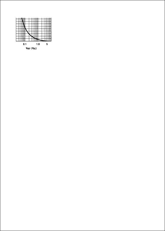
Typical Performance Characteristics
|
Linearity Error vs. VREF |
Unadjusted Offset Error vs. VREF Voltage |
Voltage |
00558344
00558343 |
|
Linearity Error vs. Temperature |
Linearity Error vs. fCLK |
00558345 |
00558346 |
Power Supply Current vs. Temperature (ADC0838, |
|
ADC0831, ADC0834) |
Output Current vs. Temperature |
00558348
00558347
Note: For ADC0832 add IREF.
ADC0831/ADC0832/ADC0834/ADC0838
7 |
www.national.com |
ADC0831/ADC0832/ADC0834/ADC0838
Typical Performance Characteristics (Continued)
Power Supply Current vs. fCLK
00558329
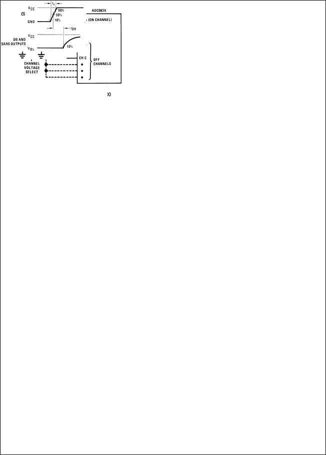
Leakage Current Test Circuit
00558303
TRI-STATE Test Circuits and
Waveforms
t1H
00558349
t0H
00558350
t1H
00558351
t0H
00558352
www.national.com |
8 |
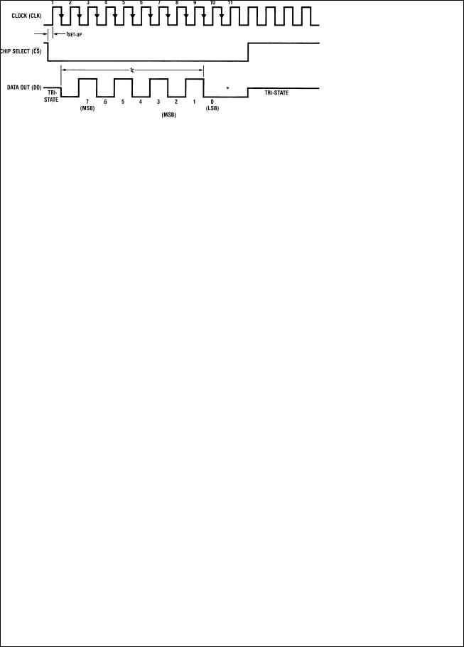
Timing Diagrams
Data Input Timing |
Data Output Timing |
00558324 |
00558325 |
ADC0831 Start Conversion Timing
00558326
ADC0831 Timing
00558327
*LSB first output not available on ADC0831.
ADC0831/ADC0832/ADC0834/ADC0838
9 |
www.national.com |

ADC0831/ADC0832/ADC0834/ADC0838
Timing Diagrams (Continued)
ADC0832 Timing
00558328
ADC0834 Timing
00558305
www.national.com |
10 |
 Loading...