


5962-8765401FA
54FCT138
1-of-8 Decoder/Demultiplexer
General Description
The FCT138 is a high-speed 1-of-8 decoder/demultiplexer.
This device is ideally suited for high-speed bipolar memory
chip select address decoding. The multiple input enables allow parallel expansion to a 1-of-24 decoder using just three
FCT138 devicesora 1-of-32 decoder using four FCT138 devices and one inverter.
Features
n Demultiplexing capability
n Multiple input enable for easy expansion
n Active LOW mutually exclusive outputs
n Outputs sink capability of 32mA, source capability of
12mA
n TTL input and output level compatible
n CMOS power consumption
n Standard Microcircuit Drawing (SMD) 5962-8765401
Ordering Code
Military Package Package Description
Number
54FCT138DMQB J16A 16-Lead Ceramic Dual-In-Line
54FCT138FMQB W16A 16-Lead Cerpack
54FCT138LMQB E20A 20-Lead Ceramic Leadless Chip Carrier, Type C
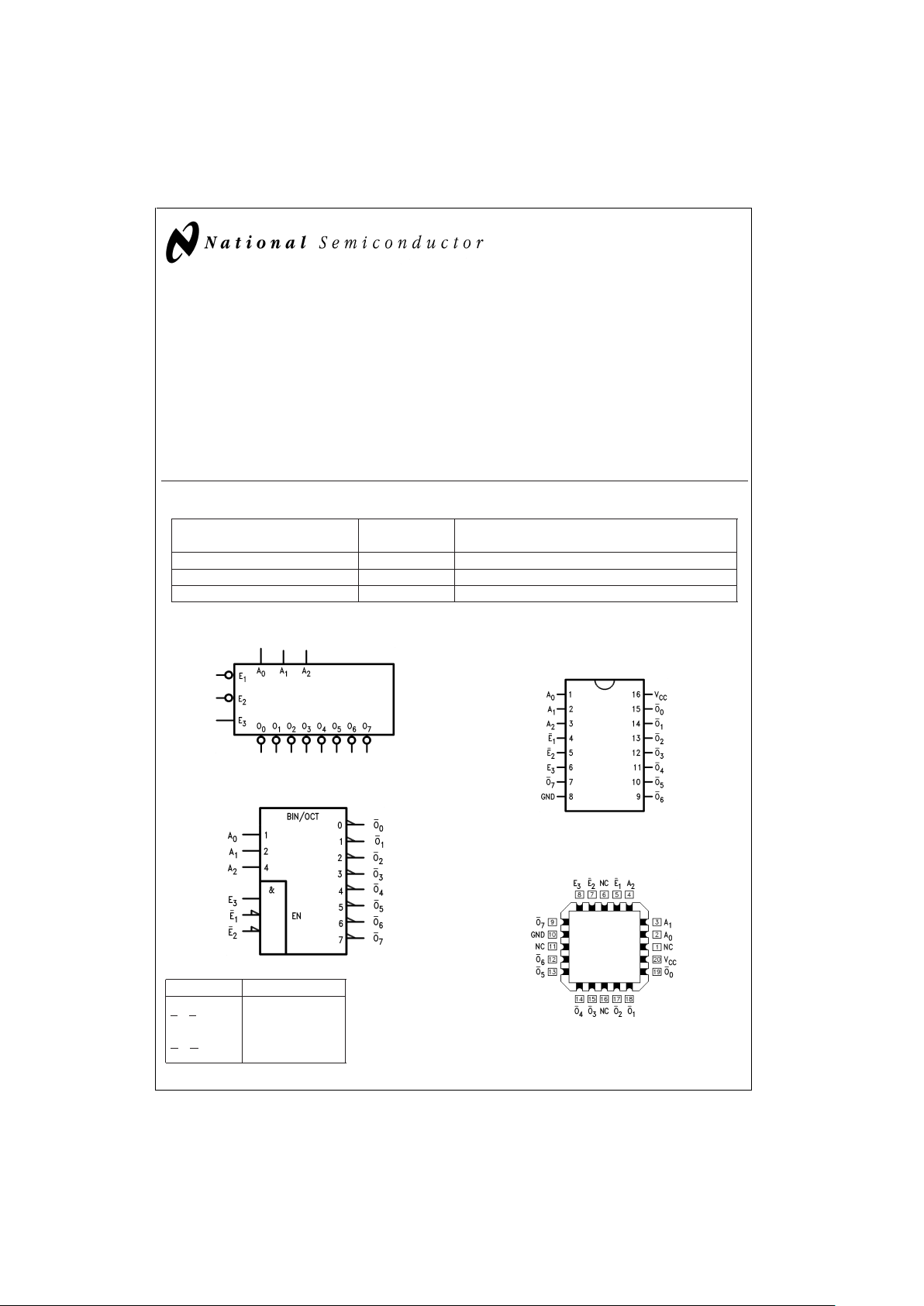
Logic Symbols
Pin Names Description
A
0–A2
Address Inputs
E
1–E2
Enable Inputs
E
3
Enable Input
O
0–O7
Outputs
Connection Diagrams
FACT®is a registered trademark of Fairchild Semiconductor Corporation.
DS100963-1
IEEE/IEC
DS100963-7
Pin Assignment
for DIP and Flatpak
DS100963-2
Pin Assignment
for LCC
DS100963-3
October 1999
54FCT138 1-of-8 Decoder/Demultiplexer
© 1999 National Semiconductor Corporation DS100963 www.national.com
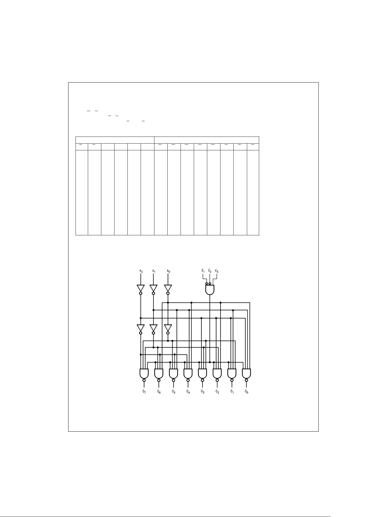
Functional Description
The FCT138 high-speed 1-of-8 decoder/demultiplexer accepts three binary weighted inputs (A
0,A1,A2
) and, when
enabled, provides eight mutually exclusive active-LOW outputs (O
0–O7
). The FCT138 features three Enable inputs,
two active-LOW (E1,E2) and one active-HIGH (E3). All outputs will be HIGH unless E1and E2are LOW and E3is
HIGH. This multiple enable function allows easy parallel ex-
pansion of the device to a 1-of-32 (5 lines to 32 lines) decoder with just four FCT138 devices and one inverter (see
Figure 1
). The FCT138 can be used as an 8-output demultiplexer by using one of the active LOW Enable inputs as the
data input and the other Enable inputs as strobes. The Enable inputs which are not used must be permanently tied to
their appropriate active-HIGH or active-LOW state.
Inputs Outputs
E
1E2E3A0A1A2O0O1O2O3O4O5O6O7
HXXXXXHHHHHHHH
XHXXXXHHHHHHHH
XXLXXXHHHHHHHH
LLHLLLLHHHHHHH
LLHHLLHLHHHHHH
LLHLHLHHLHHHHH
LLHHHLHHHLHHHH
LLHLLHHHHHLHHH
LLHHLHHHHHHLHH
LLHLHHHHHHHHLH
LLHHHHHHHHHHHL
H=HIGH Voltage Level
L=LOW Voltage Level
X=Immaterial
Logic Diagram
DS100963-4
Please note that this diagram is provided only for the understanding of logic operations and should not be used to estimate propagation delays.
54FCT138
www.national.com 2
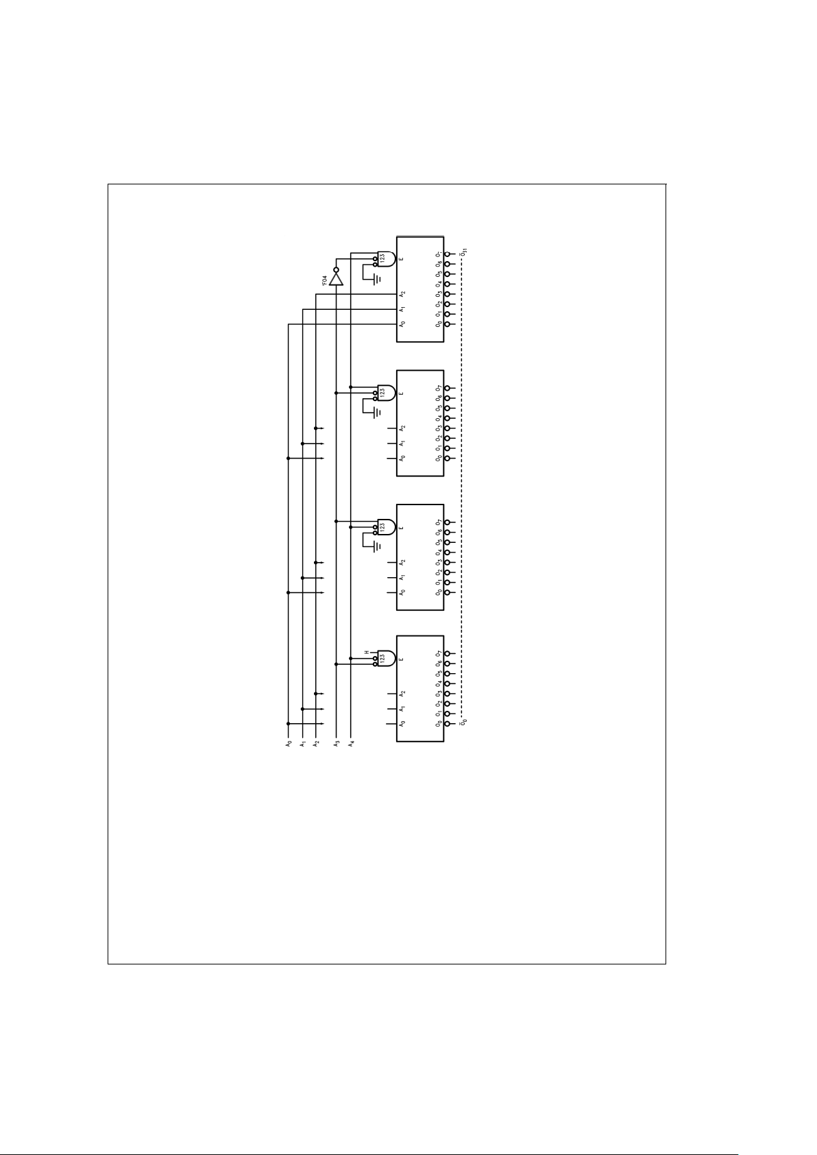
Logic Diagram (Continued)
DS100963-5
FIGURE 1. Expansion to 1-of-32 Decoding
54FCT138
www.national.com3
 Loading...