


September 1998
54AC153 · 54ACT153 Dual 4-Input Multiplexer
General Description
The 'AC/'ACT153 is a high-speed dual 4-input multiplexer with common select inputs and individual enable inputs for each section. It can select two lines of data from four sources. The two buffered outputs present data in the true (non-inverted) form. In addition to multiplexer operation, the 'AC/'ACT153 can act as a function generator and generate any two functions of three variables.
Features
nICC reduced by 50%
nOutputs source/sink 24 mA
n'ACT153 has TTL-compatible inputs
nStandard Microcircuit Drawings (SMD)
Ð'AC153: 5962-87625
Ð'ACT153: 5962-87698
Logic Symbols
IEEE/IEC
DS100271-1
DS100271-2
|
|
|
|
Pin |
Description |
|
|
|
|
Names |
|
|
|
|
|
|
|
|
I0a±I3a |
Side A Data Inputs |
|||
|
I0b±I3b |
Side B Data Inputs |
|||
|
S0, S1 |
Common Select |
|||
|
|
|
|
|
Inputs |
|
|
a |
Side A Enable Input |
||
|
|
E |
|
||
|
|
Side B Enable Input |
|||
|
E |
b |
|||
|
Za |
Side A Output |
|||
|
Zb |
Side B Output |
|||
FACT® is a registered trademark of Fairchild Semiconductor Corporation.
Multiplexer Input-4 Dual 54ACT153 · 54AC153
© 1998 National Semiconductor Corporation |
DS100271 |
www.national.com |
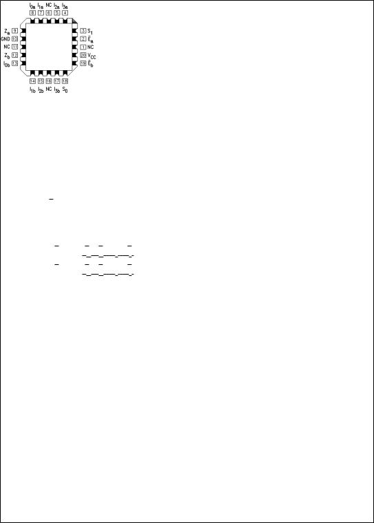
Connection Diagrams
Pin Assignment |
Pin Assignment |
for DIP and Flatpak |
for LCC |
DS100271-3
Functional Description
The 'AC/'ACT153 is a dual 4-input multiplexer. It can select two bits of data from up to four sources under the control of the common Select inputs (S0, S1). The two 4-input multiplexer circuits have individual active-LOW Enables (Ea, Eb) which can be used to strobe the outputs indepedently. When the Enables (Ea, Eb) are HIGH, the corresponding outputs Za, Zb) are forced LOW. The 'AC/'ACT153 is the logic implementation of a 2-pole, 4-position switch, where the position of the switch is determined by the logic levels supplied to the Select inputs. The logic equations for the outputs are shown below.
Za = Ea · (I0a · S1 · S0 + I1a · S1 · S0 +
I2a · S1 · S0 + I3a · S1 · S0)
Zb = Eb · (I0b · S1 · S0 + I1b · S1 · S0 +
I2b · S1 · S0 + I3b · S1 · S0)
|
|
|
|
|
|
|
DS100271-4 |
|
|
|
Truth Table |
|
|
|
|
|
|
||||
|
|
|
|
|
|
|
|
|
|
|
Select |
|
|
|
Inputs (a or b) |
|
Output |
||||
Inputs |
|
|
|
|
|
|
|
|
|
|
|
|
|
|
|
|
|
|
|
|
|
S0 |
S1 |
|
E |
|
I0 |
I1 |
I2 |
|
I3 |
Z |
X |
X |
H |
X |
X |
X |
|
X |
L |
||
L |
L |
|
L |
L |
X |
X |
|
X |
L |
|
L |
L |
|
L |
H |
X |
X |
|
X |
H |
|
H |
L |
|
L |
X |
L |
X |
|
X |
L |
|
H |
L |
|
L |
X |
H |
X |
|
X |
H |
|
L |
H |
|
L |
X |
X |
L |
|
X |
L |
|
L |
H |
|
L |
X |
X |
H |
|
X |
H |
|
H |
H |
|
L |
X |
X |
X |
|
L |
L |
|
H |
H |
|
L |
X |
X |
X |
|
H |
H |
|
|
|
|
|
|
|
|
|
|
|
|
H = HIGH Voltage Level
L = LOW Voltage Level
X = Immaterial
www.national.com |
2 |

Logic Diagram
DS100271-5
Please note that this diagram is provided only for the understanding of logic operations and should not be used to estimate propagation delays.
3 |
www.national.com |
 Loading...